
Rf Sputtering Diagram
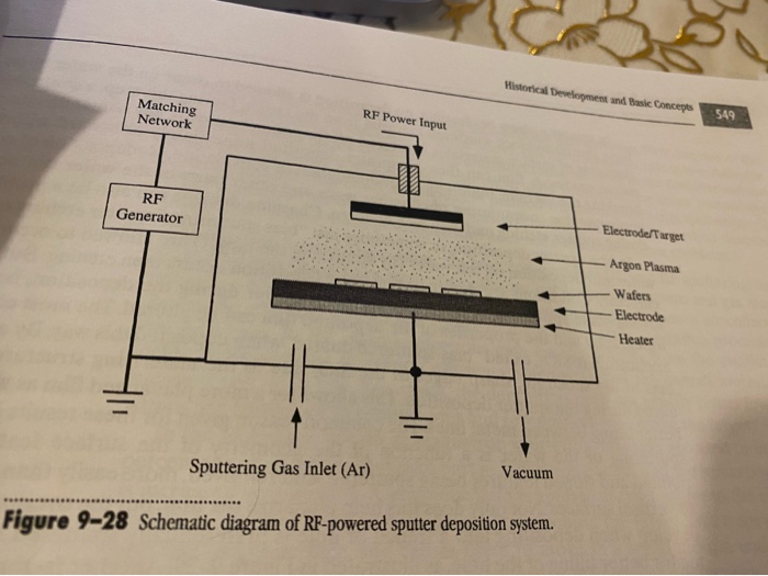
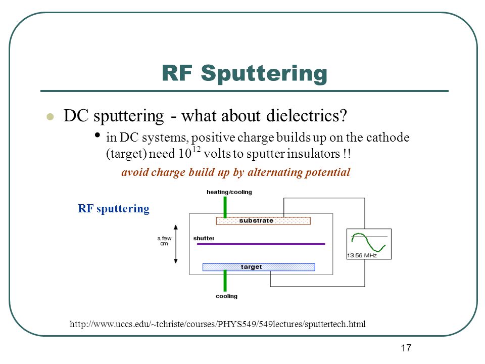
The sputtering of materials by radio frequency fields is generally known and is discussed in an article by J L Vossen appearing in the Journal of Vacuum Science and Technology, Vol 8, No 5, Sept/Oct 1971 Deposition of a thin film by RF bias sputtering is achieved in a vacuum ionization chamber which is typically a metallic housing.

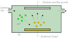
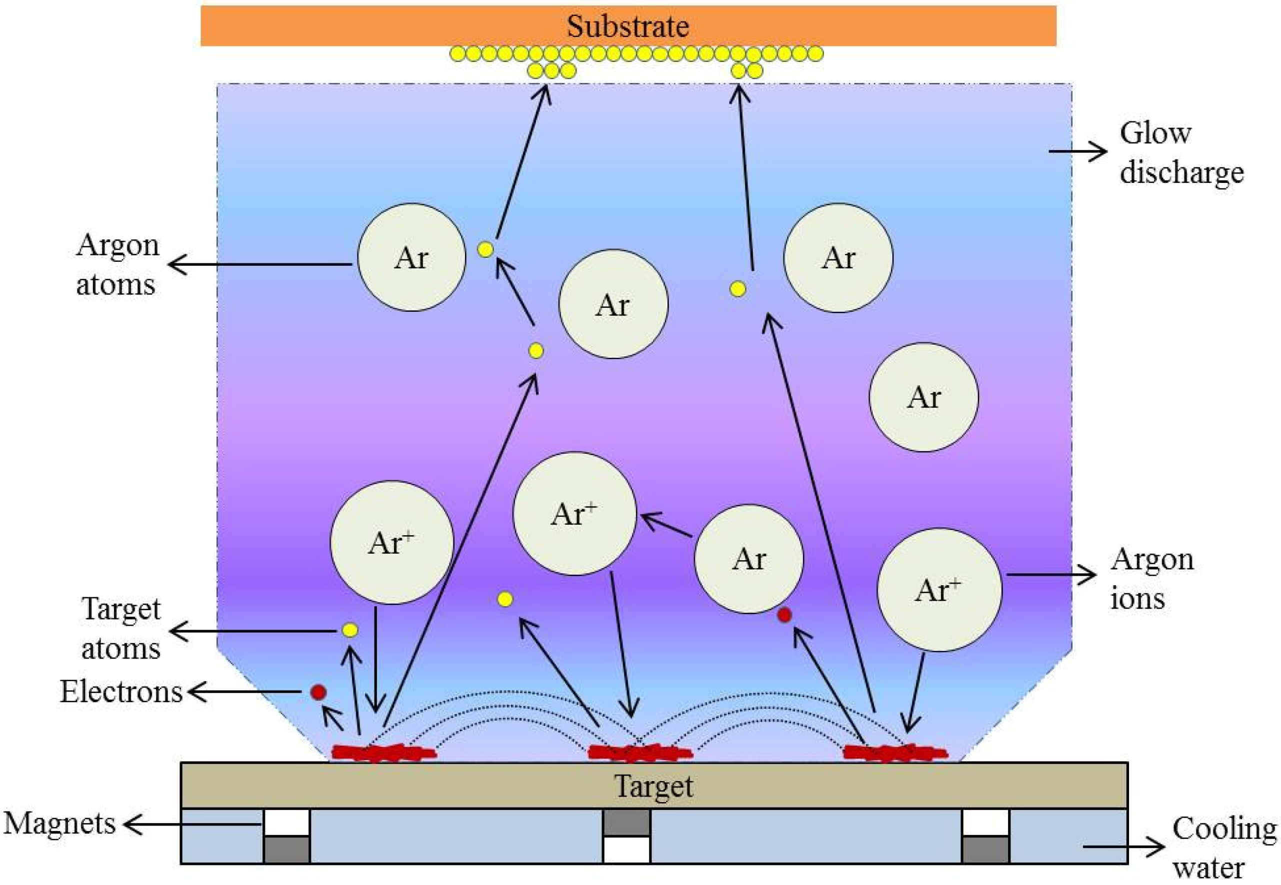
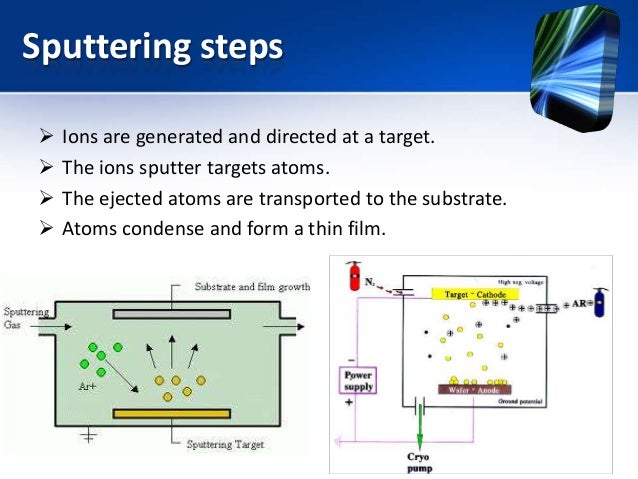
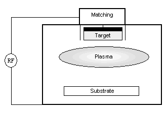
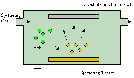
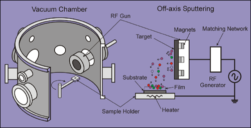
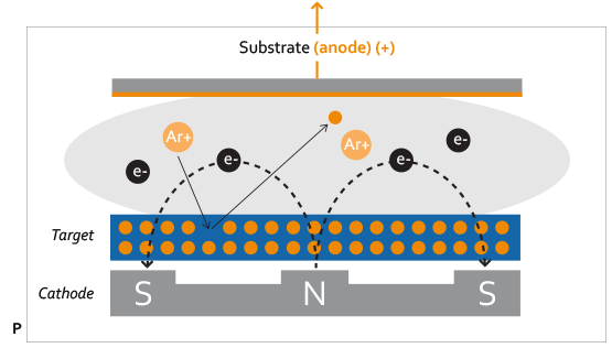
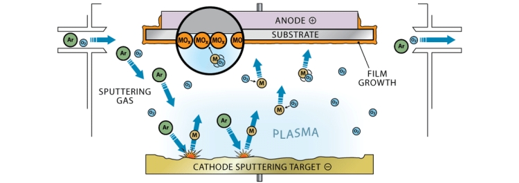
Rf sputtering diagram. Sputter deposition is a physical vapor deposition (PVD) method of thin film deposition by sputteringThis involves ejecting material from a "target" that is a source onto a "substrate" such as a silicon wafer Resputtering is reemission of the deposited material during the deposition process by ion or atom bombardment Sputtered atoms ejected from the target have a wide energy distribution. RF sputtering (Cont 2) The induced negative biasing of the target due to RF powering means that continuous sputtering of the target occurs throughout the RF cycle But it is also means that this occurs at both electrodes 42 RF sputtering (Cont 3) The wafer will be sputtered at the same rate as the target since the voltage drops would be the. Comparative Study of MgSi Films Deposited by DC and RF Glow Discharge Sputtering Substrate loading tray Fig1 Schematic diagram of glow discharge sputtering system used in this study Fig2 Photograph of targets composed of Mg and Si with area ratio of MgSi=25% 75% (a) and =50%50% (b).
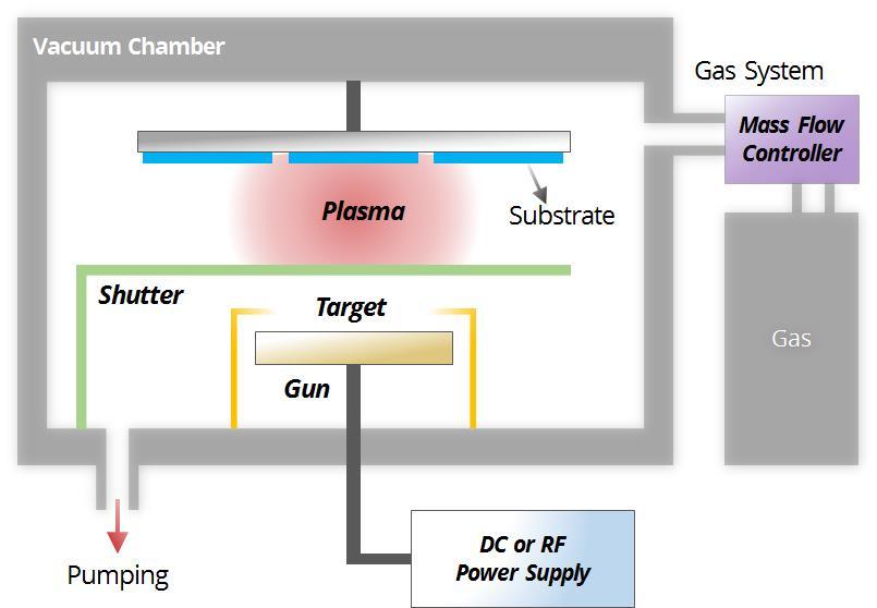
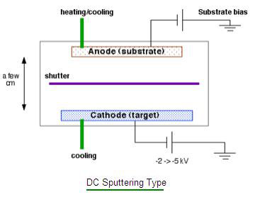
Sputtering (RF sputtering Advantages (Easier to keep plasma going under Sputtering (RF sputtering Advantages, DC sputtering, Magnetron Sputtering, RF sputtering, Comparison between RF,DC and Magnetron). Saturation point atoms added as point defects 5 • Nitrogen already a part of the target in the CVC System chamber 5 Diagram of RF Sputtering including Substrate Bias Source 4 24 Design Approach N2 Ar Gas Ratio SM Kang, et al, showed that increased presence of N2 gas in chamber increases sheet resistance. Refer to FIG 1 which is a crosssectional diagram of a sputtering apparatus in which the invention is embodied A sputtering device, either RF diode sputtering or DC magnetron sputtering, has a low pressure inert gas chamber (100).
Fig 3 Closeup of sputtering module in open position showing details of sputtering chamber Film thickness monitor can be seen at shutter opening, A TeAs main target is mounted on pedestal for "sputterup" configuration 14 Fig 4 Block diagram of vacuum and gasflow systems 16 Fig 5 Design details of substrate holder 25 Fig 6. When sputtering Aluminum and Copper alloys, the film on the wafer has more copper than the target Reason At the target, the argon has achieved high enough energy to sputter the Al and Cu evenly However, in the gas (lower electric field), the heavier atoms are less effected by light sputter gas The light Al can gain enough energy to be. Sputtering (RF sputtering Advantages (Easier to keep plasma going under Sputtering (RF sputtering Advantages, DC sputtering, Magnetron Sputtering, RF sputtering, Comparison between RF,DC and Magnetron).
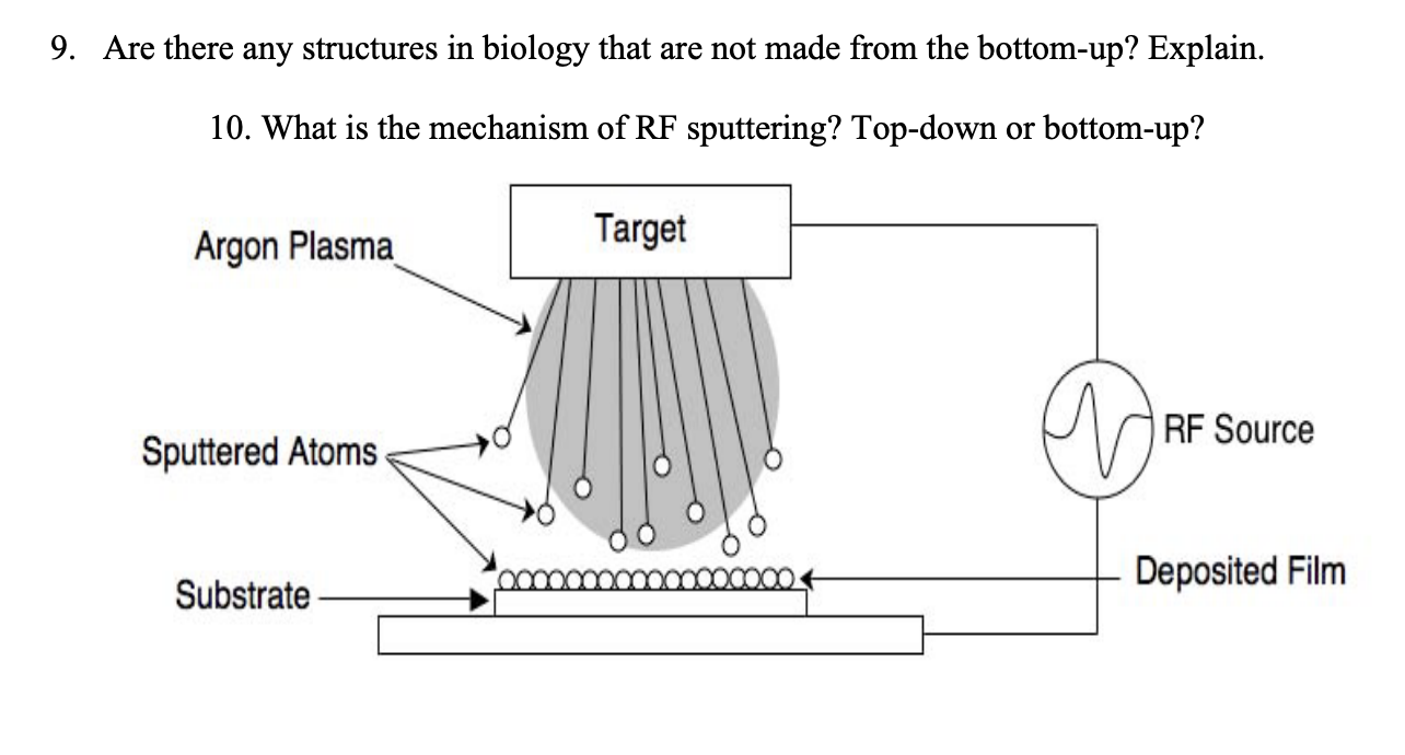
Diagram of the RF Sputtering Process As with DC Sputtering, RF Sputtering runs an energetic wave through an inert gas in a vacuum chamber which becomes ionized The target material or cathode which is to become the thin film coating is bombarded by these high energy ions sputtering off atoms as a fine spray covering the substrate to be coated. Atom transport model in Secs III,. Printed circuit boards are awesome You basically draw the schematic diagram onto the printed circuit board, which is coated with a goldlike film, then dunk it in a liquid for awhile, causing the film to sputter or etch away, until all that you are left with is an etched circuit – no wires, no mess.
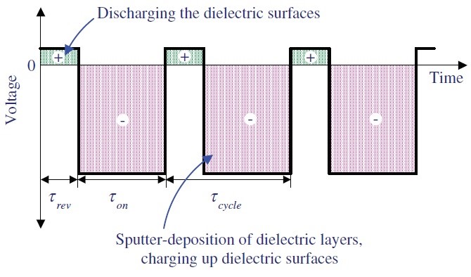
Schematic diagram of RF sputtering RF, Radiofrequency When negative potential is applied to the target, it is bombarded by positive ions and since the target is insulating, the positive charge keeps on building on the target until it repels any further positive bombardment Later during the positive half of the cycle, it is bombarded by. A device and method for sputtering dielectric targets, for reactive sputtering, and for sputter etching, including a target, anode and auxiliary electrode where each of the foregoing elements is electrically isolated from a grounded chamber containing a plasma and during a sputtering cycle, the anode and target are connected across a first floating power supply which applies a first series of. 25a The relative position of rf loop, cathode, and the probe units 34 25b Structure of sputtering unit including the Helmholtz coils 36 26a Schematical diagram of electrical network for measurement of Langmuir probe characteristics, include a rf filter circuit 37 26b Photograph showing the instrumentation for the.
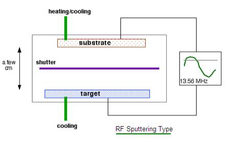
V The Effect of Hydrogen on the Optical, Structural Properties and the Crystallization of GeTe 2 Thin Films Prepared by RF Magnetron Sputtering Ke Cao ABSTRACT Thin films of GeTe 2 were deposited on glass substrates using RF magnetron sputtering with various hydrogen flow rates in the growth chamber. Figure 3 Diagram of a "cool" sputtering head The overall result is a low mean voltage head with low energy input The possibility of thermal damage due to radiant heating and electron bombardment is considered negligible For a typical modern magnetron sputter coater Vacuum 8 x l02 to 2 x l02 mbar Sputtering Voltage 100V to 3Kv. A schematic diagram of an RF diode sputter chamber is shown in Figure 1 The chamber depicted in this figure represents the essential elements of a Perkins Elmer 2400 sputtering system Copper was chosen for this study because it is commonly used as the conducting layer in.
Since the target acts as electrode in DC mode of sputter deposition, the target or source material must be conductive Therefore, Al, Ti, W, Silicide and other metals can be sputtered this way To deposit nonconductors like oxides, nitrides, lightly doped silicon, other methods like RF or AC sputtering is used. MAGNETRON SPUTTERING OF MULTICOMPONENT REFRACTORY THIN FILMS A Dissertation in multidimensional phase diagrams pose a few important questions what are the metal stoichiometries 3 Exploring High Power Pulsed Radio Frequency (RF) Magnetron Sputtering 128 Appendix A Supplementary Data for the Properties of RF Sputtered. Figure 3 Diagram of a "cool" sputtering head The overall result is a low mean voltage head with low energy input The possibility of thermal damage due to radiant heating and electron bombardment is considered negligible For a typical modern magnetron sputter coater Vacuum 8 x l02 to 2 x l02 mbar Sputtering Voltage 100V to 3Kv.
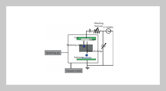
RF powder sputtering t TO RF SUPPLY Figure 1 Block diagrams of the RF sputtering system with the important accessories a Conventional and b Modified (1target, 2cathode shield, 3plasma region, 4anode (substrate holder), 5argon gas inlet, 6RF tuning network, 7gasoutlet, 8coolant water) smaller by reducing the argon gas pressure. Thin films were deposited by magnetron radiofrequency (RF) magnetron sputtering using a Co 175 Fe 125 O 4 ceramic target, which has been elaborated from mechanical mixture of Co 3 O 4 and Fe 3 O 4 commercial powders The powder mixture was pressed in a die and the green disc ( cm in diameter and 5 mm thick) was slowly heated to eliminate. RF Generators and Matching Networks 100, 300, 600, 1000 and 00 Watt 1356 MHz RF generators for sputtering and RF biasing DC Generators 750 W and 1500 W continuous DC generators with integral 4 way switchboxes.
RF sputtering (Cont 2) The induced negative biasing of the target due to RF powering means that continuous sputtering of the target occurs throughout the RF cycle But it is also means that this occurs at both electrodes 42 RF sputtering (Cont 3) The wafer will be sputtered at the same rate as the target since the voltage drops would be the. I RF Generator Leading RF plasma control for process precision and reliability Benefit from fast, seamless process transitions and advanced pulsing Learn More DC Power Supply Wide power delivery, precise control, pulsed DC and advanced arc management system enable complex sputtering processes. A horizontal RFsputtering system based on a planar magnetron have been used in this work for the deposition of HfB 2 films, designed to use standard round targets with A schematic diagram of the sputtering system is shown in Fig 1 AA GONCHAROV, AN YUNDA ET AL J NANO ELECTRON PHYS 10, (18) RF generator 1356 MHz C.
Basic sputtering process diagram Page 2 Nanomaterials applications Page 3 University of Tulsa sputtering apparatus Page 3 RF sputter deposition has many practical uses both in industrial and scientific applications In the field on Nanotechnology, working with small objects to achieve the desired pattern of deposition and. For RF sputtering, a highfrequency generator is used generating electromagnetic power in the MHzRegion (typical 1356 MHz) The output voltage and current capabilities of these generators are limited, so they need to work on a defined load impedance of 50 W. 34 Schematic E vs x band diagram of the Al/HfO2/SiO2/ptype Si structure in this (100) substrates using reactive RF sputter deposition Substrate temperature and the amount of oxygen used during deposition were varied to determine their effect on leakage current and microstructure Xray diffraction (XRD) and atomic force.
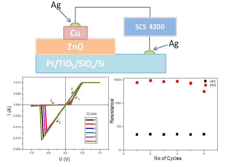
Schematic diagram of indig enously designed locally fabricated RF magnetron sputtering system It consists of a cylind rical process chamber coupled with a TMP followed by a roughing pump which yi. I RF Generator Leading RF plasma control for process precision and reliability Benefit from fast, seamless process transitions and advanced pulsing Learn More DC Power Supply Wide power delivery, precise control, pulsed DC and advanced arc management system enable complex sputtering processes. I used RF sputtering for the Pt bottom electrode (~300 nm), PLD for HfO 2 (~50 nm), and Ebeam evaporation for the top electrodes with a shadow mask.
All that is seen with a practical sputtering system are the negative glow and the dark spaces adjacent to the electrodes, (diagram B) In practice, DC diode sputtering is seldom used industrially and the field is dominated by DC magnetron sputtering for the deposition of metals RF Diode Sputtering Why use RF?. In RF sputtering there are a cathode (the target) and a anode, in series with a blocking capacitor (C) The capacitor is part of an impedancematching network that proves the power transfer from the RF source to the plasma discharge The power supply is a high voltage RF source often fixed at 1356 MHz The blocking capacitor C is placed in the. Schematic diagram of magnetron sputtering Magnetron sputtering is the collision process between incident particles and targets Since highspeed sputtering is performed at a low pressure, it is necessary to effectively increase the ionization rate of the gas (DC) magnetron sputtering and radio frequency (RF) magnetron sputtering, each has.
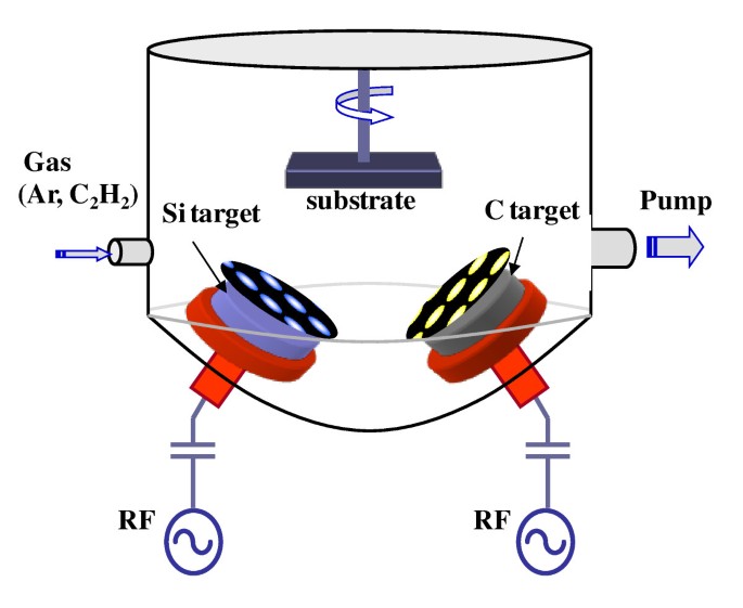
Using a combination process of rf sputtering and MHDPCVD Figure 1 illustrates the schematic diagram of an experimental setup sustaining two discharge plasmas in a deposition chamber The discharge plasma #1 was an rf sputtering for DLC film deposition, which was sustained with rf magnetron cathode with a 1 inch graphite target using a. SputteringCompoundsJPDc_R1doc Page 1 of 24 pages Sputtering yields of compounds using argon ions M P Seah 1 and T S Nunney 2 1Analytical Science Division, National Physical Laboratory, Teddington, Middlesex TW11 0LW, UK, 2Thermo Fisher Scientific, The Birches Industrial Estate, Imberhorne Lane, East Grins tead, West Sussex RH19 1UB, UK emails martinseah@nplcouk and timnunney@thermofishercom. In this video I am discussing about the sputtering (DCRF) for thin film deposition.
Describe the rf diode sputtering process for metal thinfilm fabrication and the reactorscale models of interest We then develop and show relevant results for the fluid flow model, the plasma model, the sputter model, and the direct simulation Monte Carlo ~DSMC!. Schematic diagram of RF magnetron sputtering system used in this work Gas inlet with mass flow meter was used to supply argon into the main chamber The vacuum in the main chamber was established by a mechanical rotary pump and a turbo molecular pump Moreover, a load lock chamber was employed to protect the vacuum condition in the main chamber. RF Generators and Matching Networks 100, 300, 600, 1000 and 00 Watt 1356 MHz RF generators for sputtering and RF biasing DC Generators 750 W and 1500 W continuous DC generators with integral 4 way switchboxes.
Since the target acts as electrode in DC mode of sputter deposition, the target or source material must be conductive Therefore, Al, Ti, W, Silicide and other metals can be sputtered this way To deposit nonconductors like oxides, nitrides, lightly doped silicon, other methods like RF or AC sputtering is used. The sputtering of materials by radio frequency fields is generally known and is discussed in an article by J L Vossen appearing in the Journal of Vacuum Science and Technology, Vol 8, No 5, Sept/Oct 1971 Deposition of a thin film by RF bias sputtering is achieved in a vacuum ionization chamber which is typically a metallic housing. RF sputtering (Cont 2) The induced negative biasing of the target due to RF powering means that continuous sputtering of the target occurs throughout the RF cycle But it is also means that this occurs at both electrodes 42 RF sputtering (Cont 3) The wafer will be sputtered at the same rate as the target since the voltage drops would be the.
Rf RF voltage divider circuit 𝑉 𝑓≈1114∗𝑉𝑂 V rf amplitude of RF discharge voltage V O amplitude of measured RF voltage 𝑽𝒓𝒇≈𝟕𝟏∗𝑽𝑶 Theoretical Actual measurement Incorrect values on capacitors and inductors 0 10 3010 0 10 30 h = 0 cm h = 25 cm h = 50 cm V p (V) RF power (W) Dependence of V p. A schematic diagram of an RF diode sputter chamber is shown in Figure 1 The chamber depicted in this figure represents the essential elements of a Perkins Elmer 2400 sputtering system at Nonvolatile Electronics (NVE) where all the experiments were performed Copper was chosen. Silver oxide (A 2 O) films were deposited on glass and silicon substrates held at temperatures in the range 303–473 K by reactive RF magnetron sputtering of silver target The films formed at room temperature were single phase Ag 2 O with polycrystalline in nature, while those deposited at 373 K were improved in the crystallinity.
To learn more, explore DC magnetron sputtering, RF magnetron sputtering, and pulsed DC sputtering (links below) Magnetron sputtering is available in a variety of source configurations and compatible with many of Angstrom’s process control capabilities and advanced fixturing options. I used RF sputtering for the Pt bottom electrode (~300 nm), PLD for HfO 2 (~50 nm), and Ebeam evaporation for the top electrodes with a shadow mask. Saturation point atoms added as point defects 5 • Nitrogen already a part of the target in the CVC System chamber 5 Diagram of RF Sputtering including Substrate Bias Source 4 24 Design Approach N2 Ar Gas Ratio SM Kang, et al, showed that increased presence of N2 gas in chamber increases sheet resistance.
Using a combination process of rf sputtering and MHDPCVD Figure 1 illustrates the schematic diagram of an experimental setup sustaining two discharge plasmas in a deposition chamber The discharge plasma #1 was an rf sputtering for DLC film deposition, which was sustained with rf magnetron cathode with a 1 inch graphite target using a. I RF Generator Leading RF plasma control for process precision and reliability Benefit from fast, seamless process transitions and advanced pulsing Learn More DC Power Supply Wide power delivery, precise control, pulsed DC and advanced arc management system enable complex sputtering processes. Schematic diagram of ixdiode sputtering process chamber Figure 2 Typical variation of mean free path with pressure Pressure (Pal 102 102 100 102 104 68 Sputtering m m c cathode until it reaches the dark space the plasma extinguishes ions cease to be produced and sputter.
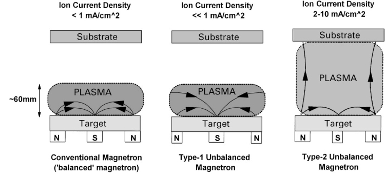
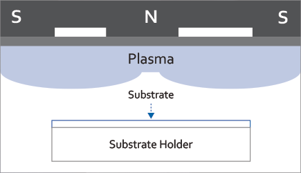
Rf sputtering can be used with a magnetic field in balanced and unbalanced configurations to obtain a result similar to dclike diode discharge In fig 2 the different configurations of dc and rf sputtering are shown a) b) Fig 2 Sputtering configurations a) dc sputtering, b) rf sputtering. Saturation point atoms added as point defects 5 • Nitrogen already a part of the target in the CVC System chamber 5 Diagram of RF Sputtering including Substrate Bias Source 4 24 Design Approach N2 Ar Gas Ratio SM Kang, et al, showed that increased presence of N2 gas in chamber increases sheet resistance. A schematic diagram of a typical RF sputtering system is shown in the figure below Figure 6 Typical RF sputtering system Casting In this process the material to be deposited is dissolved in liquid form in a solvent The material can be applied to the substrate by spraying or spinning Once the solvent is evaporated, a thin film of the.
RF Generators and Matching Networks 100, 300, 600, 1000 and 00 Watt 1356 MHz RF generators for sputtering and RF biasing DC Generators 750 W and 1500 W continuous DC generators with integral 4 way switchboxes. Schematic diagram of ixdiode sputtering process chamber Figure 2 Typical variation of mean free path with pressure Pressure (Pal 102 102 100 102 104 68 Sputtering m m c cathode until it reaches the dark space the plasma extinguishes ions cease to be produced and sputter. RF powder sputtering t TO RF SUPPLY Figure 1 Block diagrams of the RF sputtering system with the important accessories a Conventional and b Modified (1target, 2cathode shield, 3plasma region, 4anode (substrate holder), 5argon gas inlet, 6RF tuning network, 7gasoutlet, 8coolant water) smaller by reducing the argon gas pressure.
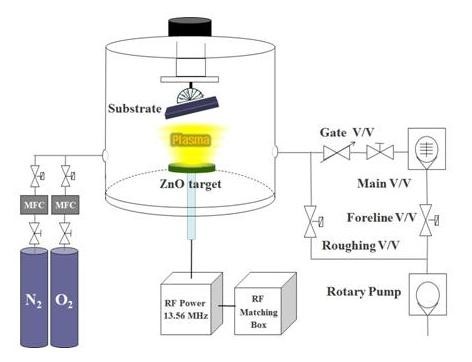
Reactive RF Magnetron Sputtering So far we have considered the deposition of materials sputtered by Argon The argon flow may also be augmented with another gas, eg Oxygen or Nitrogen Gases other than Oxygen and Nitrogen have been used in reactive sputtering including ammonia, hydrogen sulphide, hydrocarbons and Hydrogen. In order to grow Cu/In/Se stack the schematic diagram of RF sputtering system is shown in Figure 22 After evacuation of chamber to 1 × 10 − 6 torr, pure Ar is introduced into chamber to sputter target and maintain pressure of 1 × 10 − 2 torr.
Structural And Optical Properties Of A Radio Frequency Magnetron Sputtered Zno Thin Film With Different Growth Angles Springerlink
Magnetron Sputtering Types Of Coating Processes And Advantages

Rf Sputtering Principles Ifn Trento
Rf Sputtering Diagram のギャラリー
Rf Substrate Bias With High Power Impulse Magnetron Sputtering Hipims Diagram Schematic And Image 03

A Schematic Diagram Of Facing Target Rf Magnetron Sputt Open I
Iopscience Iop Org Article 10 1149 2 jss Pdf
Reactive Sputtering Deposition Presentation
Q Tbn And9gcrmgxpgzucw S3sp1bixoax2godwfl3pff9llex4tglrv55bg8c Usqp Cau

Line 22f1fa19c3m1b7c8e13c9c6d3p38d19d7b34 Rf Sputtering Plasma Zno Signals 5g Wow Seti Alien Space Science News

Schematic Diagram Of The Ar Gas Rf Magnetron Sputtering System Download Scientific Diagram
Sputter Deposition Wikipedia
Cens Main
Q Tbn And9gcrs4t5gdkz1ormcnktha6w4d Cb6uby8bir Jwcoybrpe Zmzh8 Usqp Cau
Http Www Davidpublisher Com Public Uploads Contribute 55cbfb4f4cfa8 Pdf

Rf Sputtering Principles Ifn Trento
Coatings Free Full Text Recent Developments In R F Magnetron Sputtered Thin Films For Ph Sensing Applications An Overview Html
Q Tbn And9gcqrrma6pky5 U7sohjkjyiiokgbcikxhutol4ab7etg5jamztgg Usqp Cau

Nano Point Nanotechnology Sputtering

1 Schematic Drawing Of A Rf Sputtering System Adapted From 92 Download Scientific Diagram

Fabrication Of Oriented Hydroxyapatite Film By Rf Magnetron Sputtering Aip Advances Vol 7 No 8
Sputtering Process

Radio Frequency Sputtering An Overview Sciencedirect Topics
Advances In Rf Sputtering Aultimut

Optimization Of Sputtering Parameters For The Deposition Of Low Resistivity Indium Tin Oxide Thin Films
Phenotypic Expression Of Human Endothelial Cells Grown Onto Stent Material Coated With Titanium Ti Compounds Journal Of Applied Science And Engineering

Compact 300w Auto Matched Rf Generator For Diy Plasma Coating With Optional Magnetron Sputtering Gun
Thickness Distribution Of Sputtered Films On Curved Substrates For Adjustable X Ray Optics

What Is Dc Sputtering

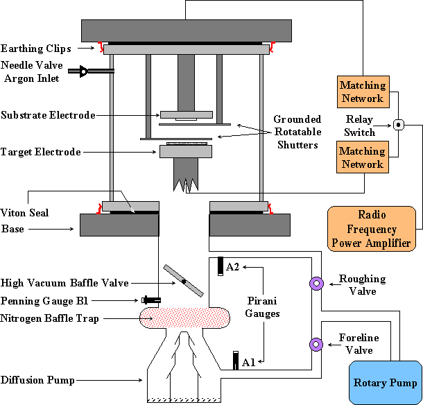
Diode Sputtering Description Nordiko Technical Service Ltd

Optimization Of Sputtering Parameters For The Deposition Of Low Resistivity Indium Tin Oxide Thin Films
Rf Dc Sputtering Source For 4 X 0 25 Target St40 Demaco

Rf Sputtering Principles Ifn Trento
Sputter Deposition Wikipedia

Temperature Effects On Vo2 Thin Films Deposited By Rf Sputtering For The Degradation By Photocatalysis Of Methylene Blue And Naproxen In International Journal Of Chemical Reactor Engineering Volume 18 Issue 7

Figure 1 Schematic Diagram Of The Rf Magnetron Sputtering Chamber

Diagram The Schematic Diagram Of Dc Magnetron Sputtering Diagram Full Version Hd Quality Sputtering Diagram Speakerdiagram Asandria It

Difference Between Rf Sputtering And Dc Sputtering Rf Sputtering Vs Dc Sputtering
Pulsed Dc Magnetron Sputtering Dc Sputtering Process Vaccoat
Technical Research Centre Trc
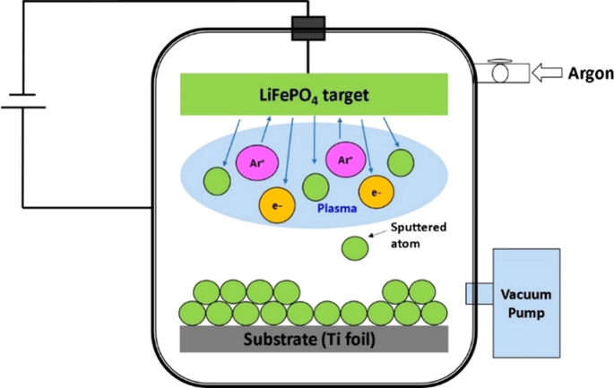
Sputtered Porous Li Fe P O Film Cathodes Prepared By Radio Frequency Sputtering For Li Ion Microbatteries Scientific Reports
Http Www Phys Sinica Edu Tw Tigp Nano Course 14 Spring Classnote Nanometer Thin film Pdf
More About Rf Sputtering

Figure 39 3 Schematic Of Rf Sputtering Chamber

Clipboard No 1 May 10
Solved 9 Are There Any Structures In Biology That Are No Chegg Com
Dc Sputtering Vs Rf Sputtering The Comparison Of Dc Sputtering And Rf Sputtering
Effect Of Deposition Time On Sputtered Zno Thin Films And Their Gas Sensing Application Springerlink
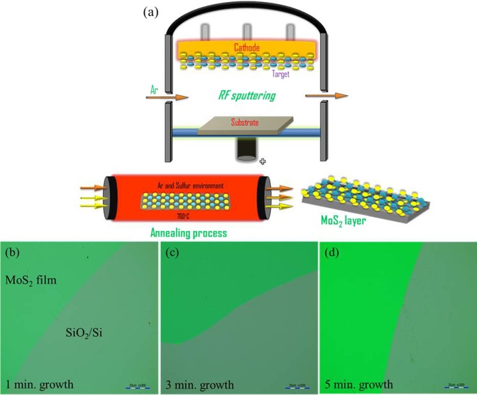
Large Area Continuous And High Electrical Performances Of Bilayer To Few Layers Mos 2 Fabricated By Rf Sputtering Via Post Deposition Annealing Method Scientific Reports
3 0 General Experimental Techniques Growth And Study Of Magnetostrictive Fesibc Thin Films For Device Applications
Core Ac Uk Download Pdf Pdf

Rf Power Packages For Sputtering Plasma Manitou Systems Inc

Rf Power Packages For Sputtering Plasma Manitou Systems Inc

Faq Vaccoat
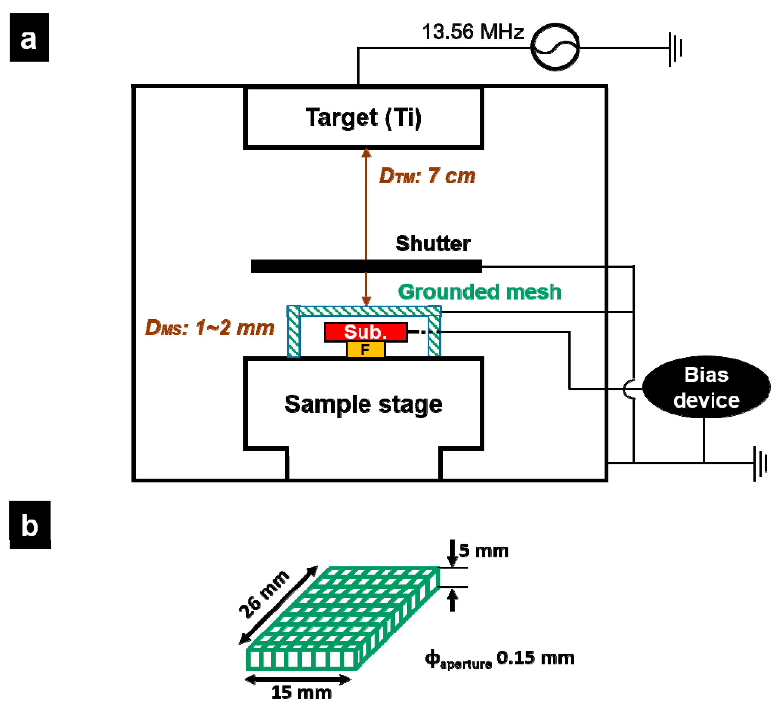
Coatings Free Full Text Generation Of Charged Ti Nanoparticles And Their Deposition Behavior With A Substrate Bias During Rf Magnetron Sputtering Html
Iopscience Iop Org Article 10 1149 2 jss Pdf
2

A Schematic Diagram Of The Radiofrequency Rf Sputtering System For Download Scientific Diagram
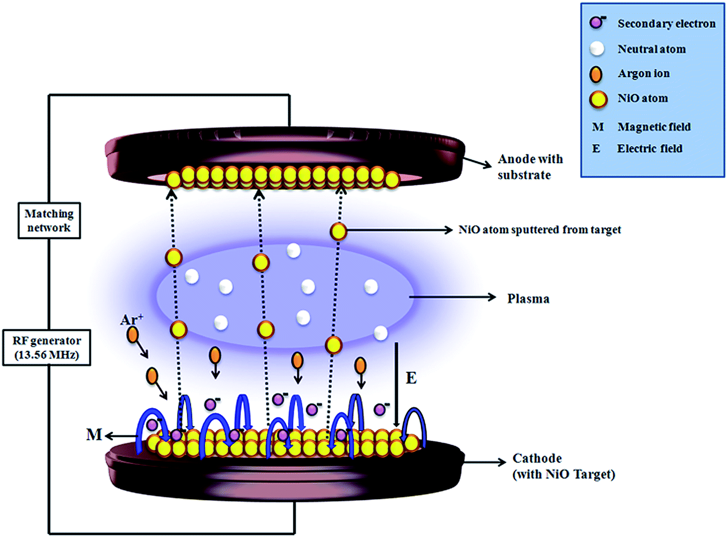
Improved Electrochromic Performance Of A Radio Frequency Magnetron Sputtered Nio Thin Film With High Optical Switching Speed Rsc Advances Rsc Publishing Doi 10 1039 C5rae

Hybrid Pvd Coater In Glove Box 2 Rf Sputtering 2 Evaporation Source Vtc H3 Gb
Solved Hello In Rf Sputtering Deposotion Why We Designe Chegg Com

Faq Vaccoat

A Schematic Diagram Of Rf Magnetron Sputtering System Download Scientific Diagram
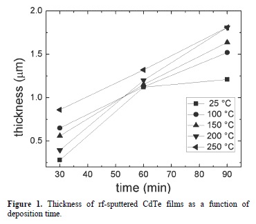
Effects Of Temperature And Deposition Time On The Rf Sputtered Cdte Films Preparation
Content Sciendo Com Downloadpdf Journals Msp 35 2 Article P374 Pdf

Influence Of The Substrate Bias Voltage On The Crystallographic Structure And Surface Composition Of Ti6a14v Thin Films Deposited By Rf Magnetron Sputtering
Magnetron Sputtering Deposition Systems Denton Vacuum

Sputter Deposition An Overview Sciencedirect Topics
Dc Sputtering Vs Rf Sputtering The Comparison Of Dc Sputtering And Rf Sputtering
Sic Formation For A Solar Cell Passivation Layer Using An Rf Magnetron Co Sputtering System Nanoscale Research Letters Full Text

What Is Rf Sputtering
Rf Dc Low Profile Sputtering Source For 2 X 0 12 Magnetic Target St Mm Lp Demaco
Q Tbn And9gcs2a964ydtwatkuz Vymtbxlsevfzsvb4m7wbszgbz9ovnapjpv Usqp Cau
Www Diva Portal Org Smash Get Diva2 Fulltext01 Pdf
Osa Optoelectronic Properties And Anisotropic Stress Of Mo Zno Thin Films Deposited On Flexible Substrates By Radio Frequency Magnetron Sputtering
Www Osapublishing Org Oe Viewmedia Cfm Uri Oe 28 8 Seq 0

Sputtering Configurations A Dc Sputtering B Rf Sputtering Download Scientific Diagram

Dr Shabbir A Bashar S Ph D Thesis Chapter 3 Section 2
Www Ias Ac In Article Fulltext Sadh 034 04 0543 0556
Physical Properties Of Rf Sputtered Zns And Znse Thin Films Used For Double Heterojunction Zns Znse Cdte Photovoltaic Structures Applied Surface Science X Mol

Sputtered Hydroxyapatite Nanocoatings On Novel Titanium Alloys For Biomedical Applications Intechopen

Objectives Template

Rf Sputtering Applications Ifn Trento

Rf Sputtering Of Polycrystalline 100 002 And 101 Oriented Aln On An Epitaxial 3c Sic 100 On Si 100 Substrate Journal Of Vacuum Science Technology B Vol 32 No 6
Sputtering Processes For Thin Film Deposition Ppt Video Online Download

Figure 2 Characteristics Of Bilayer Molybdenum Films Deposited Using Rf Sputtering For Back Contact Of Thin Film Solar Cells

Research Center For Magnetic And Spintronic Materials

Rf Sputtering Applications Ifn Trento

Figure 3 From Ferroelectric Hf 0 5 Zr 0 5 O 2 Films By Rf Sputtering Method Semantic Scholar

The Effect Of Substrate Roughness On The Properties Of Rf Sputtered Azo Thin Film Mrs Communications Cambridge Core
Magnetron Sputtering Deposition Systems Denton Vacuum

1 Schematic Diagram Of Radio Frequency Rf Sputtering System From Download Scientific Diagram
Deposition Processes
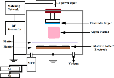
Figure 1 Study Of Structural And Electrical Properties Of Zno Thin Film For Thin Film Transistor Tft Applications Springerlink

Sciencecentral

Rf Sputtering Principles Ifn Trento
Gale Academic Onefile Document Characteristics Of Bilayer Molybdenum Films Deposited Using Rf Sputtering For Back Contact Of Thin Film Solar Cells

Cylindrical And Rotating Magnetron Sputtering Vacuum Technology Coating Blog

Sputtering Type An Overview Sciencedirect Topics
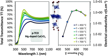
P Type Conducting Transparent Characteristics Of Delafossite Mg Doped Cucro2 Thin Films Prepared By Rf Sputtering Journal Of Materials Chemistry C Rsc Publishing
Magnetron Sputtering Types Of Coating Processes And Advantages
Figure 1 Align Ag Nanorods Via Oxidation Reduction Growth Using Rf Sputtering
Coatings Free Full Text The Effect Of Rf Sputtering Conditions On The Physical Characteristics Of Deposited Gegan Thin Film Html

Impact Of Plasma Electron Flux On Plasma Damage Free Sputtering Of Ultrathin Tin Doped Indium Oxide Contact Layer On P Gan For Ingan Gan Light Emitting Diodes Son 18 Advanced Science Wiley Online
Http Www Sfu Ca Gchapman E495 E495l9l Pdf


