
Rf Sputtering Process
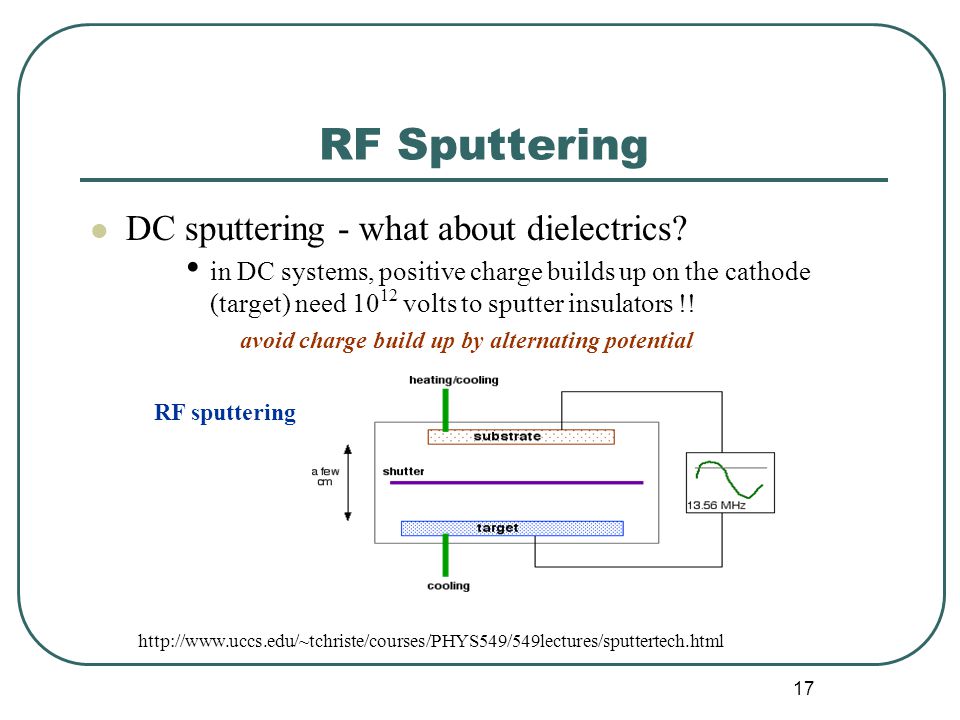
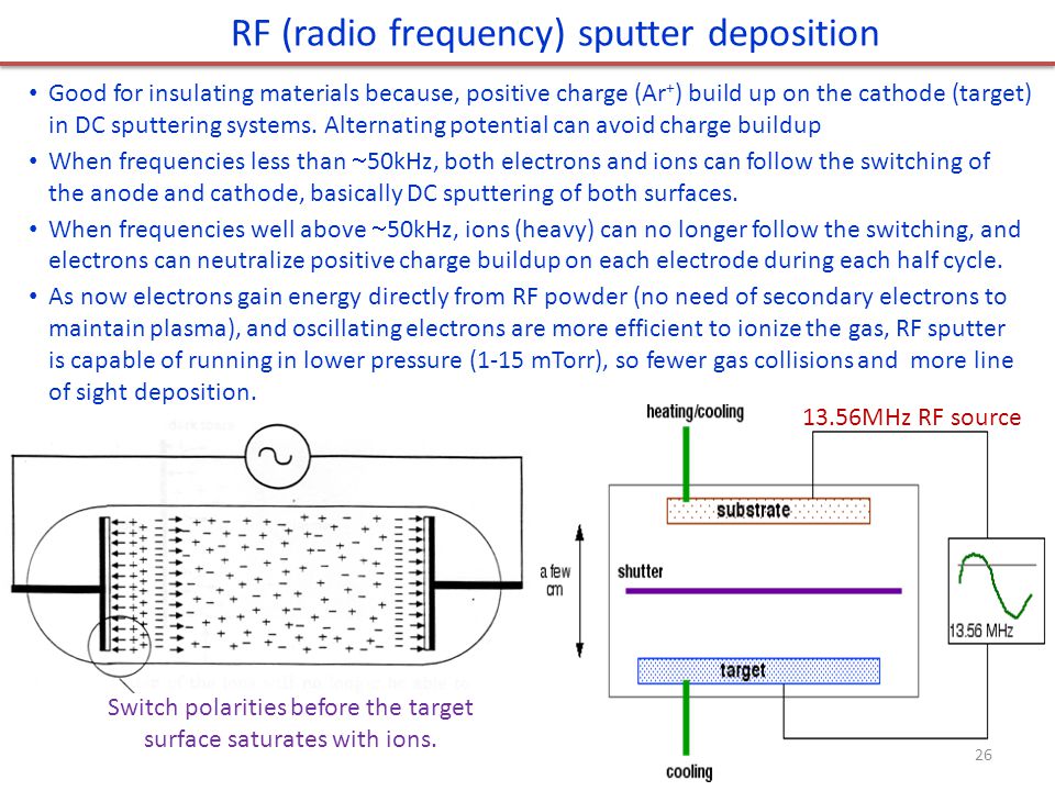
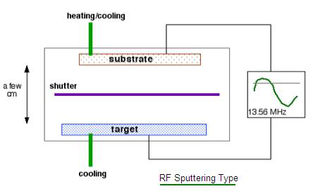
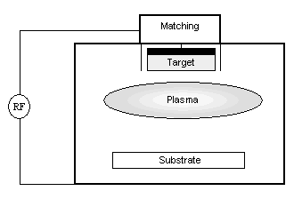
To continue the process, the polarity must be reversed to attract enough electrons from the plasma to eliminate surface charge This periodic reversal of polarity is done automatically by applying a radiofrequency (RF) voltage on the target assembly Thus, this type of sputtering is known as “RF sputtering”, (figure 2).
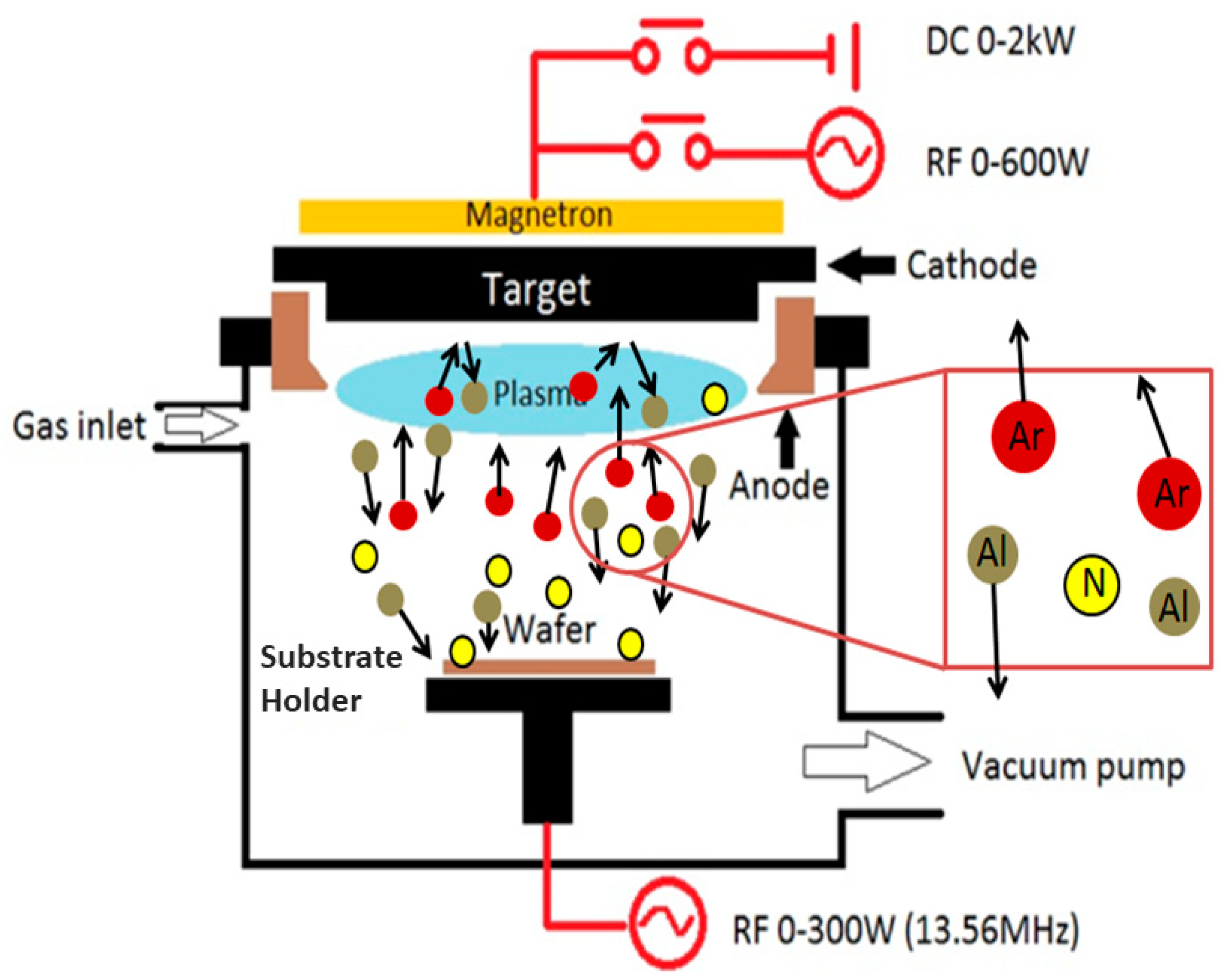
Rf sputtering process. RF Diode sputtering technology, newly developed updated on an old technology works even better, because it does not need magnetic confinement and provides optimum coating uniformity It provides a very flat target erosion with no racetrack, no poisoning of the target, little or no arching and a more stable process. Magnetron sputtering is the collision process between incident particles and targets Since highspeed sputtering is performed at a low pressure, it is necessary to effectively increase the ionization rate of the gas. Although more expensive, RF sputtering can be used to deposit almost any material Ar is used as the process gas because it is inert and relatively inexpensive, but gases such as O 2 and N 2 can be introduced to deliberately react with the sputtered material to deposit oxides and nitrides for example.
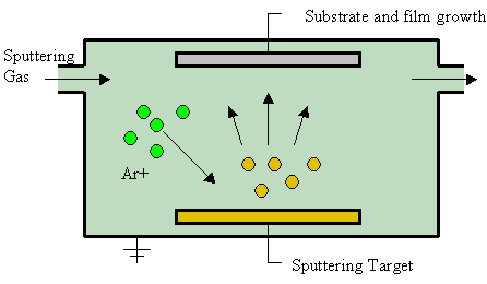
PZT thin film was fabricated by using RFsputtering process, and platinum was used as bottom electrodes The sputtering gases were Ar:O2=25:0 sccm, Ar:O2=:5 sccm, or Ar:O2=15:10 sccm After sputtering, the PZT film was annealed for 5 minutes under O2 gas environment and at the temperature of 600 0C, 650 0C, 700 0C or 750 0C. Physical Vapor Deposition (PVD) by Sputtering Physical Vapor Deposition (PVD) is a process by which a thin film of material is deposited on a substrate according to the following sequence of steps 1) the material to be deposited is converted into vapor by physical means;. Rf magnetron is a cold process, and hence will be more useful, comapred to rf diode which causes heating effects on the substrate where samples are fixed for coating.
DC, RF, HiPIMS, Pulsed DC Reactive, nonreactiv, codeposition Polyteknik has build up an extensive knowledge of the sputtering process from inhouse coating and complex build systems We support our customers in the range from small scale advanced R&D process development to full scale customised production systems Polyteknik has experience with a wide range of sputtering processes including. Sputtering is a versatile form of physical vapor deposition which can be used to deposit coatings of conductive or insulating materials It uses ionized gas to ablate (“sputter”) a target to create a thin film of that material on a substrate. Sputtering – additional methods • • • • • Reactive & Non reactive sputtering RF & DC sputtering Magnetron sputtering Collimated sputtering IonBeam sputtering 22 Applications Of Thin Film Technology Microelectronics CPU processors, cell phones, ipod, watches, batteries, Solar Panels 23.
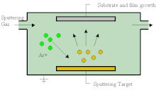
Sputtering Sputtering is a technology in which the material is released from the source at much lower temperature than evaporation The substrate is placed in a vacuum chamber with the source material, named a target, and an inert gas (such as argon) is introduced at low pressure. And 3) the vapor undergoes. RF Diode sputtering technology, newly developed updated on an old technology works even better, because it does not need magnetic confinement and provides optimum coating uniformity It provides a very flat target erosion with no racetrack, no poisoning of the target, little or no arching and a more stable process.
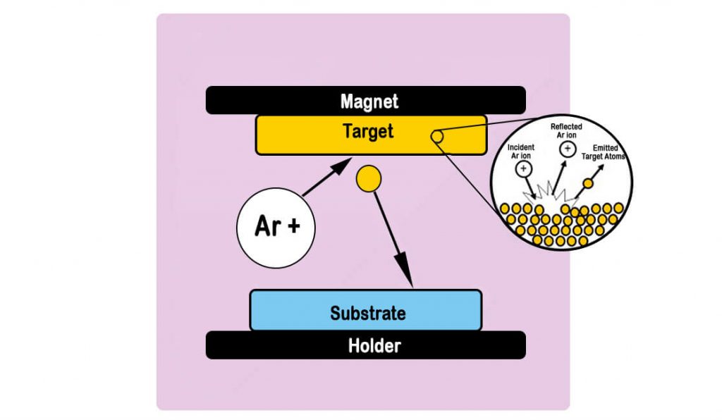
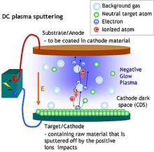
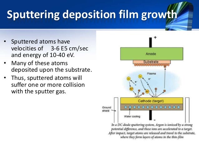
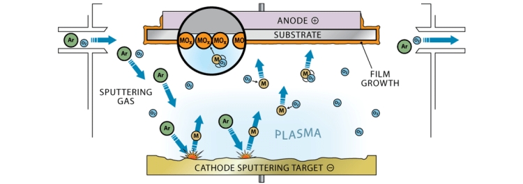
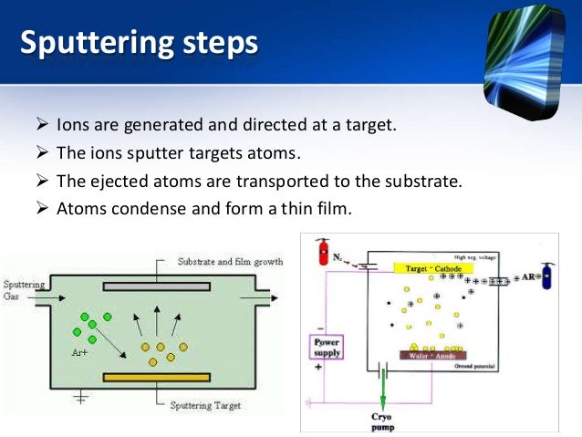
A sputter etch process will always require more RF power than an RF bias (only) process The substrate stage and its components will need to withstand the higher RF power and current flow – resulting in higher heating of the stage’s components Which RF Power control mode is used during the RF bias process ?. The sputtering process occurs when the target material is bombarded with the sputtering gas and the resulting energy transfer causes target particles to escape, travel and deposit on the substrate as a film For the sputtering process to produce an effective coating, a number of criteria must be met. In fact, sputtering is the transferring momentum process of incident particles (usually ions of inert gases), to the collision surface Some parameters such as power, angle, and the mass of particles incident, as well as binding energy between the atoms are effective in efficiency.
PVD RF Sputtering coating principle Magnetron Sputter Deposition Process Animation PVD RF Sputtering coating principle Magnetron Sputter Deposition Process Animation Please note that if you are under 18, you won't be able to access this site Are you 18 years old or above?. Sputtering is a technique used to deposit thin films of a material onto a surface (aka "substrate") By first creating a gaseous plasma and then accelerating the ions from this plasma into some source material (aka "target"), the source material is eroded by the arriving ions via energy transfer and is ejected in the form of neutral particles either individual atoms, clusters of atoms. Sputtering is a technique used to coat surfaces to improve mechanical resistance, or biocompatibility Its caracterized by introducing argon, an inert gas, w.
Sputtering Ajit Behera Fix up the target materials (Ni & Ti), Deposition & Experimental process Fix target to substrate distance, Keep the substrate in the chamber Close the chamber Set the Basevacuume Adjust Substrate temperature Set partial gas pressure, gas flow rate, substrate bias, substrate rotation Ready for Deposition For another Bilayer deposition Set the rf power Set the DC power. Although more expensive, RF sputtering can be used to deposit almost any material Ar is used as the process gas because it is inert and relatively inexpensive, but gases such as O 2 and N 2 can be introduced to deliberately react with the sputtered material to deposit oxides and nitrides for example. RF or Radio Frequency Sputtering is the technique involved in alternating the electrical potential of the current in the vacuum environment at radio frequencies to avoid a charge building up on certain types of sputtering target materials, which over time can result in arcing into the plasma that spews droplets creating quality control issues on the thin films – and can even lead to the complete cessation of the sputtering of atoms terminating the process.
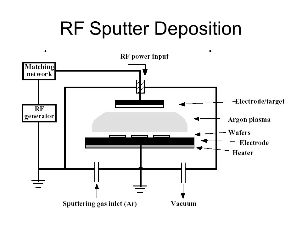
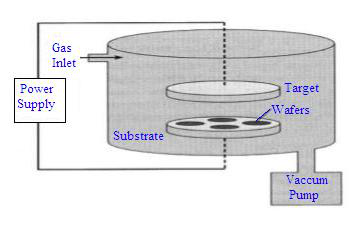
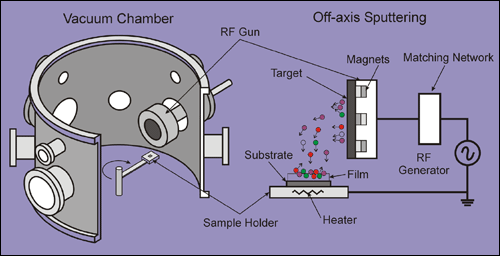
In RF sputtering, coexcitation of the power source is desired to prevent RF mode beating The deposition of thin films is carried out by a cosputtering cathode technique particularly suited for deposition of doped thin films on large area substrates A relatively large planar magnetron sputtering apparatus having a rectangular (picture frame. Radio frequency (RF) sputtering is a technique that is used to create thin films, such as those found in the computer and semiconductor industry Like direct current (DC) sputtering, this technique involves running an energetic wave through an inert gas to create positive ions. 2) the vapor is transported across a region of low pressure from its source to the substrate;.
PVD RF Sputtering coating principle Magnetron Sputter Deposition Process Animation PVD RF Sputtering coating principle Magnetron Sputter Deposition Process Animation Please note that if you are under 18, you won't be able to access this site Are you 18 years old or above?. The object of the reactive sputtering process is to create thin films of closely controlled stoichiometry and structure Over the past decade much progress has been made developing reactive DC processes that offer much higher deposition rates when compared to RF sputtering of the bulk materials. Sputtering – additional methods • • • • • Reactive & Non reactive sputtering RF & DC sputtering Magnetron sputtering Collimated sputtering IonBeam sputtering 22 Applications Of Thin Film Technology Microelectronics CPU processors, cell phones, ipod, watches, batteries, Solar Panels 23.
PVD RF Sputtering coating principle Magnetron Sputter Deposition Process Animation PVD RF Sputtering coating principle Magnetron Sputter Deposition Process Animation Please note that if you are under 18, you won't be able to access this site Are you 18 years old or above?. RF Sputtering Details By avoiding a constant negative voltage on the cathode, ion buildup is prevented for insulating targets Can operate at lower pressures while still sustaining a plasma RF plasmas tend to fill the chamber as opposed to DC plasmas which are confined to the cathode. Sputtering process ablation of target P ≈ m Torr cathode anode ⊕ V ≈1kVEx v v e− Ar Cathode is “target”, source material cathode anode ⊕ V ≈1kVMostlyneutral source atoms (lots of e’s around) Target material (cathode) must be conductive or must use RF sputtering (later) Momentum transfer of Ar on cathode erodes.
Depending on the target material either RF or DC sputtering may be used During the sputtering process, the target material, substrate, and RF electrodes begin in a vacuum chamber Next, the inert gas, which is usually argon, neon, or krypton, depending on the size of the target material’s molecules, is directed into the chamber. Sputter configuration available from 16 Sputter sources in sputter up or sputter down Suitable for codeposition as well as sequential deposition Customize combination available base on process requirement. M any sputterPVD coatings of interest are compounds They could be deposited by cosputtering from multiple sources or by using compound targets Often the compound target material and the deposited thin film are electrically insulating making DC sputtering and substrate biasing unsuitable, so RF sputtering must be used instead.
Reactive Sputtering Reactive sputtering is a process that allows compounds to be deposited by introducing a reactive gas (typically oxygen or nitrogen) into the plasma which is typically formed by an inert gas such as argon (most common), xenon, or krypton. 6 Sputtering – General • Sputtering is a term used to describe the mechanism in which atoms are ejected from the surface of a material when that surface is stuck by sufficiency energetic particles • First discovered in 1852, and developed as a thin film deposition technique by Langmuir in 19. A Sm thin film was deposited on cleaned Si substrate by using TF 450 PVD RF sputtering system Prior to the sputtering process, the sputter chamber, substrate holder, target holder, and shutter were cleaned with acetone Then, the Sm target was fixed into the target holder, while the cleaned Si wafers were placed on the substrate holder.
A process for controlling the dihydride and monohydride bond densities in hydrogenated amorphous silicon produced by reactive rf sputtering of an amorphous silicon target There is provided a chamber with an amorphous silicon target and a substrate therein with the substrate and the target positioned such that when rf power is applied to the. RF Diode sputtering technology, newly developed updated on an old technology works even better, because it does not need magnetic confinement and provides optimum coating uniformity It provides a very flat target erosion with no racetrack, no poisoning of the target, little or no arching and a more stable process. Sputtering is a momentum transfer process in which atoms from a cathode/target are driven off by bombarding ions Sputtered atoms travel until they strike a substrate, where they deposit to from the desired layer.
Sputtering is a slower process relatively For oxide target it becomes more complicated You cannot apply higher powers, the targets loos oxygen stoichiometric, makeing large area targets is a costly affair, and demand good bonding with metallic plates for cooling. Sputtering Process Sputtering Deposition Method In terms of physics, Sputtering is a phenomenon in which energetic particles of plasma or gas hit the surface of a solid and microscopic particles are separated from it This phenomenon occurs naturally in outer space and can cause unwanted surface wear in high precision conditions. RF Diode sputtering technology, newly developed updated on an old technology works even better, because it does not need magnetic confinement and provides optimum coating uniformity It provides a very flat target erosion with no racetrack, no poisoning of the target, little or no arching and a more stable process.
Sputtering is the process whereby atoms or molecules of a material are ejected from a target by the bombardment of highenergy particles However, main disadvantages of diode sputtering were related to the very low deposition rates and large cost. Our sputter process has been designed to deposit ultraclean metal and dielectric films All wafer processing, including metal deposition, is performed inside our class 100 cleanroom An insitu RF etch is added to the process to insure good film adhesion and ohmic contact to underlying conductive layers. Radio frequency magnetron sputtering, also called RF magnetron sputtering is a process that is used to make thin film, especially when using materials that are nonconductive In this process, a thin film is grown on a substrate that is placed in a vacuum chamber.
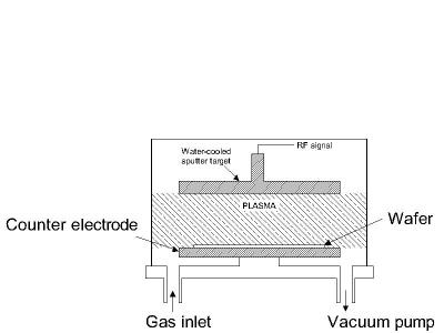
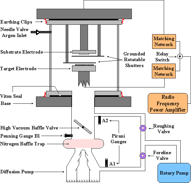
A schematic diagram of a typical RF sputtering system is shown in the figure below Figure 6 Typical RF sputtering system Casting In this process the material to be deposited is dissolved in liquid form in a solvent The material can be applied to the substrate by spraying or spinning Once the solvent is evaporated, a thin film of the. Sputtering process ablation of target P ≈ m Torr cathode anode ⊕ V ≈1kVEx v v e− Ar Cathode is “target”, source material cathode anode ⊕ V ≈1kVMostlyneutral source atoms (lots of e’s around) Target material (cathode) must be conductive or must use RF sputtering (later) Momentum transfer of Ar on cathode erodes. Since sputtering is a purely physical process, adding chemistry to, for example, deposit a compound layer must be done ad hoc through the addition of a reactive gas to the plasma, ie reactive sputtering.
RF sputtering A viable tool for MEMS fabrication 545 obtain highly caxis oriented films, which is a requirement for these films to be piezoelectric in nature In addition to the dielectric films, thin films of Cr, Au, Ti and Pt on silicon or glass substrates, (used for ZnO deposition) were also deposited by RF sputtering process. Sputtering Ajit Behera Fix up the target materials (Ni & Ti), Deposition & Experimental process Fix target to substrate distance, Keep the substrate in the chamber Close the chamber Set the Basevacuume Adjust Substrate temperature Set partial gas pressure, gas flow rate, substrate bias, substrate rotation Ready for Deposition For another Bilayer deposition Set the rf power Set the DC power. Since sputtering is a purely physical process, adding chemistry to, for example, deposit a compound layer must be done ad hoc through the addition of a reactive gas to the plasma, ie reactive sputtering.
Sputtering is the process whereby atoms or molecules of a material are ejected from a target by the bombardment of highenergy particles More significantly cathodic sputtering is the process discussed here and in this case the bombardment is by positive ions derived from an electrical discharge in a gas. RFsputtering is a suitable technique to fabricate optical planar waveguides and photonic microcavities operating in the visible and NIR regions Sputtering techniques are widely used in industrial process because high quality films can be obtained at low temperature substrates. RF sputtering A viable tool for MEMS fabrication 545 obtain highly caxis oriented films, which is a requirement for these films to be piezoelectric in nature In addition to the dielectric films, thin films of Cr, Au, Ti and Pt on silicon or glass substrates, (used for ZnO deposition) were also deposited by RF sputtering process.
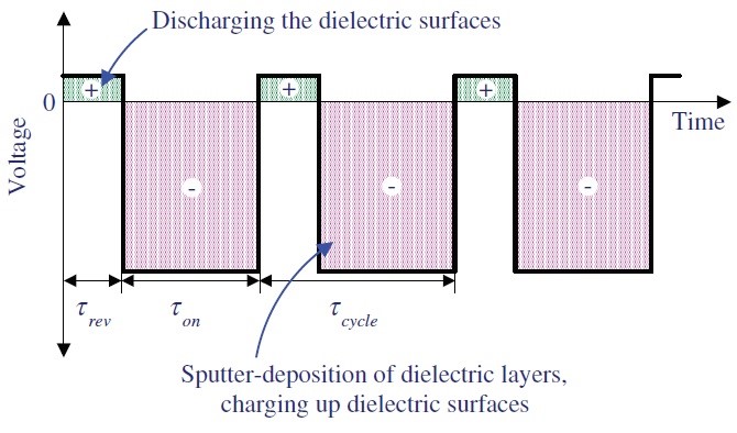
RF Sputtering Sputter deposition of insulating materials cannot be done with DC power Materials such as oxides, nitrides, and ceramics have very large DC impedance and require prohibitively high voltages to ignite and maintain a plasma Luckily, the impedance of these materials changes with the frequency of the applied power. Sputter configuration available from 16 Sputter sources in sputter up or sputter down Suitable for codeposition as well as sequential deposition Customize combination available base on process requirement. • The RF sputtering involves two processes In the first cycle, target material is negatively charged This results the polarization of atoms and the sputtering gas atoms are attracted to the source where they knock out source atoms Due to polarization, the source atoms and ionized gas ions remain on target surface.
Http//wwwperkinelmersputtercom We have been focusing on providing solutions and enhancements to PerkinElmer Sputtering Systems including PerkinElmer P. Sputtering Process, Types, and Uses Sputtering is a physical process in which atoms in a solidstate (target) are released and pass into the gas phase by bombardment with energetic ions (mainly noble gas ions). Or DC sputtering ionbeam sputtering, reactive sput tering but all these are variants of the same physi cal phenomenon Sputtering is the process whereby atoms or molecules of a material are ejected from a target by the bombardment of highenergy particles More significantly cathodic sputtering is the process.
Although more expensive, RF sputtering can be used to deposit almost any material Ar is used as the process gas because it is inert and relatively inexpensive, but gases such as O 2 and N 2 can be introduced to deliberately react with the sputtered material to deposit oxides and nitrides for example. A schematic diagram of a typical RF sputtering system is shown in the figure below Figure 6 Typical RF sputtering system Casting In this process the material to be deposited is dissolved in liquid form in a solvent The material can be applied to the substrate by spraying or spinning Once the solvent is evaporated, a thin film of the.

6 Overview Of The Basic Sputtering Process A Radio Frequency Rf Download Scientific Diagram
Combined Magnetron Sputtering And Pulsed Laser Deposition Of Tio 2 And Bfco Thin Films Scientific Reports
Thin Film Deposition Types Of Thin Films Used In Semiconductor Processing Thermal Oxides Dielectric Layers Epitaxial Layers Polycrystalline Silicon Metal Ppt Download
Rf Sputtering Process のギャラリー
Sputtering Process Sputtering Deposition Method Vaccoat

Rf Sputtering Principles Ifn Trento

Dr Shabbir A Bashar S Ph D Thesis Chapter 3 Section 2

Magnetron Sputtering An Overview Sciencedirect Topics

Sputtering Wikipedia

Faq Vaccoat

Sputter Deposition An Overview Sciencedirect Topics

Rf Sputtering Principles Ifn Trento
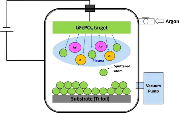
Sputtered Porous Li Fe P O Film Cathodes Prepared By Radio Frequency Sputtering For Li Ion Microbatteries Scientific Reports
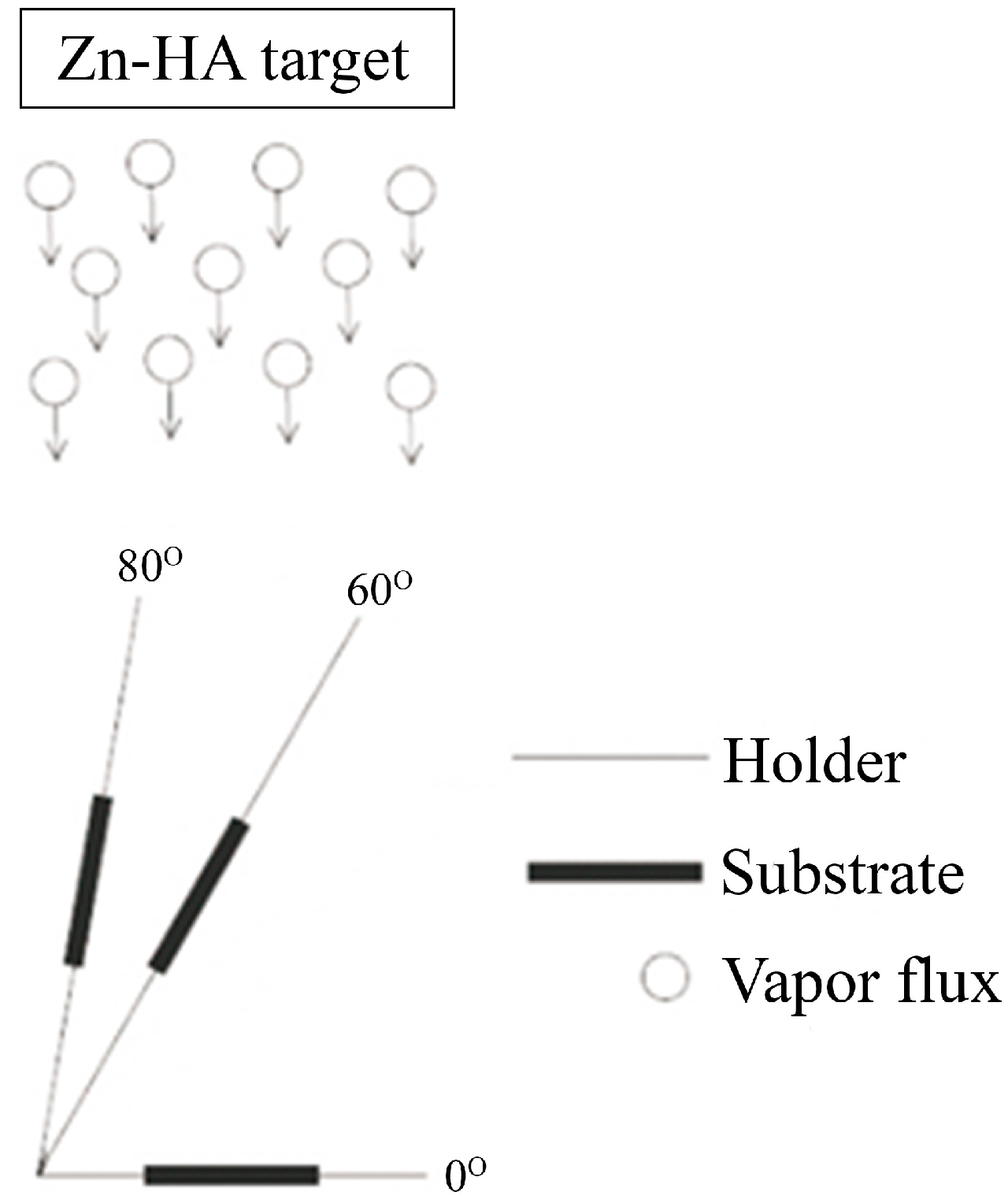
Coatings Free Full Text Glancing Angle Deposition Of Zn Doped Calcium Phosphate Coatings By Rf Magnetron Sputtering

Pdf Influence Of Reactive Sputter Deposition Conditions On Crystallization Of Zirconium Oxide Thin Films
Scientific Analytical Instruments Rf Dc Sputtering System

Rf Sputtering Principles Ifn Trento

Objectives Template

Figure 1 Align Ag Nanorods Via Oxidation Reduction Growth Using Rf Sputtering

Faq Vaccoat

Sputter Deposition Lnf Wiki
Effect Of Deposition Time On Sputtered Zno Thin Films And Their Gas Sensing Application Springerlink
Kurt J Lesker Company Combinatorial Magnetron Sputtering Advances With New Tools And New Predictive Techniques Vacuum Science Is Our Business
Www Svc Org Digitallibrary Documents 10 Spring Mmwaite Sishah Daglocker P42 50 Pdf

Schematic Of The Ito Rf Sputtering System Download Scientific Diagram

Pulsed Dc Magnetron Sputtering Dc Sputtering Process Vaccoat
Rf Magnetron Sputtering Ppt
Sputtering Processes For Thin Film Deposition Ppt Video Online Download
Q Tbn And9gcq0qx8ptyc8d016kx8jrrjkfvro2tapw6xiy2iirfojx0w8n0ll Usqp Cau

Sputtering
Thickness Distribution Of Sputtered Films On Curved Substrates For Adjustable X Ray Optics

A Schematic Diagram Of The Rf Magnetron Co Sputtering System Download Scientific Diagram
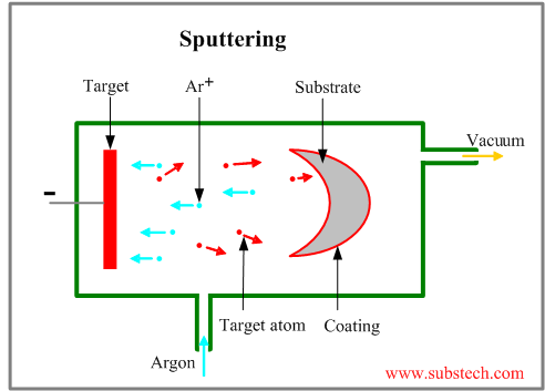
Sputtering Substech

Sputter Deposition Of Titanium And Nickel Thin Films In Radio Frequency Magnetron Discharge Characterized By Optical Emission Spectroscopy And By Rutherford Backscattering Spectrometry Sciencedirect
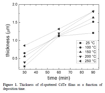
Effects Of Temperature And Deposition Time On The Rf Sputtered Cdte Films Preparation

A Schematic Diagram Of The Radiofrequency Rf Sputtering System For Download Scientific Diagram

Radio Frequency Sputtering An Overview Sciencedirect Topics
Pulsed Dc Magnetron Sputtering Dc Sputtering Process Vaccoat

Sputtering Power Induced Physical Property Variation Of Nickel Oxide Films By Radio Frequency Magnetron Sputtering
Deposition Processes

Materials Processing Using Radio Frequency Ion Sources Ion Beam Sputter Deposition And Surface Treatment Review Of Scientific Instruments Vol 90 No 2

Pvd Rf Sputtering Coating Principle Magnetron Sputter Deposition Process Animation Youtube
Q Tbn And9gcrmgxpgzucw S3sp1bixoax2godwfl3pff9llex4tglrv55bg8c Usqp Cau
Sputter Deposition Wikipedia
Indium Tin Oxide Ito Sputter Deposition Processes Springerlink
Sputtering Process

In Rf Sputtering There Are Typically A Small Area Cathode Target And Download Scientific Diagram
Nanopdf Com Download Nanometerthin Film Pdf

Pdf Comparative Study Of Ito Layers Deposited By Dc And Rf Magnetron Sputtering At Room Temperature
Www Ias Ac In Article Fulltext Sadh 034 04 0543 0556
Deposition Processes

Adnanotek Magnetron Sputtering Deposition Sputter System E Beam Evaporator Pld Pulsed Laser Deposition
3 0 General Experimental Techniques Growth And Study Of Magnetostrictive Fesibc Thin Films For Device Applications

Rf Sputtering Principles Ifn Trento

What Is Dc Sputtering
Dc Sputtering Vs Rf Sputtering The Comparison Of Dc Sputtering And Rf Sputtering
Chapter 9 Thin Film Deposition Ppt Download
Q Tbn And9gcsmv5sez6h2h0cqzl7jqe7m54c0p2spndvowf Wnheskv3v Wsg Usqp Cau

Rf Sputtering Principles Ifn Trento
More About Rf Sputtering
Dc Sputtering Vs Rf Sputtering The Comparison Of Dc Sputtering And Rf Sputtering
Akademik Adu Edu Tr Fakulte Muhendislik Personel Uploads Aozcelik Thin Film Deposition Iii Pdf

Influence Of The Substrate Bias Voltage On The Crystallographic Structure And Surface Composition Of Ti6a14v Thin Films Deposited By Rf Magnetron Sputtering

Rf Sputtering Principles Ifn Trento
Overview Of Thin Film Deposition Techniques

Compact Powder Pvd Coater With Dc Magnetron Sputtering Vibration Stage Vtc 16 Pw
Magnetron Sputtering Types Of Coating Processes And Advantages
Coatings Free Full Text Sputtering Physical Vapour Deposition Pvd Coatings A Critical Review On Process Improvement And Market Trend Demands Html
Process For Rf Sputtering Of Cadmium Telluride Photovoltaic Cell University Of Toledo Digital Repository
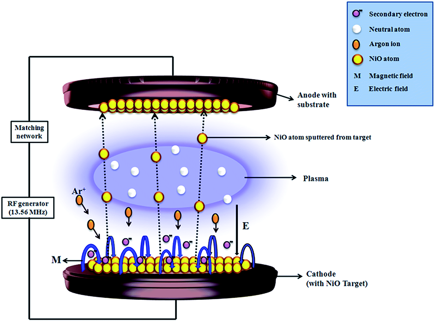
Improved Electrochromic Performance Of A Radio Frequency Magnetron Sputtered Nio Thin Film With High Optical Switching Speed Rsc Advances Rsc Publishing Doi 10 1039 C5rae
Sputter Deposition Wikipedia

Radio Frequency Magnetron Sputter Deposition As A Tool For Surface Modification Of Medical Implants Intechopen

Self Organizing Plasma Behavior In Rf Magnetron Sputtering Discharges Journal Of Applied Physics Vol 125 No

Optimization Of Sputtering Parameters For The Deposition Of Low Resistivity Indium Tin Oxide Thin Films

Pdf Structural Electrical And Optical Studies Of Zno Tio2thin Films Fabricated By Rf Sputtering Process For Uv Application Semantic Scholar

Ppt Sputtering And Cvd Pvd Technology Powerpoint Presentation Free Download Id

Pdf Structural Electrical And Optical Studies Of Zno Tio2thin Films Fabricated By Rf Sputtering Process For Uv Application Semantic Scholar

X Ray Diffraction Patterns Of Azo Films Deposited Via Rf Sputtering Download Scientific Diagram

Development Of Rf Magnetron Sputtering Method To Fabricate Pzt Thin Film Actuator Sciencedirect

Sputter Deposition An Overview Sciencedirect Topics

Pdf Determination Of Reactive Rf Sputtering Parameters For Fabrication Of Siox Films With Specified Refractive Index For Highly Reflective Siox Distributed Bragg Reflector
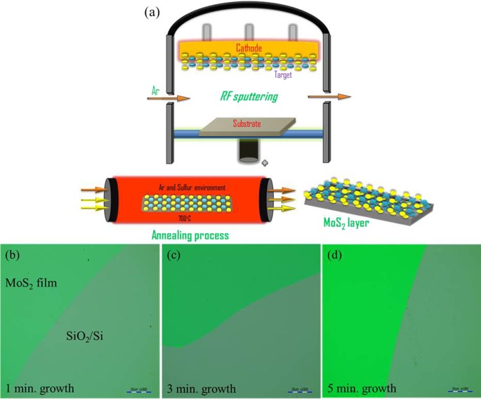
Large Area Continuous And High Electrical Performances Of Bilayer To Few Layers Mos 2 Fabricated By Rf Sputtering Via Post Deposition Annealing Method Scientific Reports

Reactive Sputtering An Overview Sciencedirect Topics
Sputtering Process

News Articles
Q Tbn And9gcrs4t5gdkz1ormcnktha6w4d Cb6uby8bir Jwcoybrpe Zmzh8 Usqp Cau

High Rate Sputtering Deposition Of Silicon Oxide Thin Films From New Sio2 Si Target Composition Journal Of Vacuum Science Technology A Vol 27 No 4
Www Mdpi Com 1996 1944 12 15 2366 Pdf
Dc Sputtering Vs Rf Sputtering The Comparison Of Dc Sputtering And Rf Sputtering

What Is Rf Sputtering
Advances In Rf Sputtering Aultimut
Sensors Free Full Text Reactive Sputtering Of Aluminum Nitride 002 Thin Films For Piezoelectric Applications A Review Html

Radio Frequency Sputtering An Overview Sciencedirect Topics
Www Svc Org Digitallibrary Documents 10 Spring Mmwaite Sishah Daglocker P42 50 Pdf
Technical Research Centre Trc

Reactive Sputtering An Overview Sciencedirect Topics

Rf Sputtering Principles Ifn Trento
Magnetron Sputtering Deposition Systems Denton Vacuum

1 Schematic Diagram Of Radio Frequency Rf Sputtering System From Download Scientific Diagram

Sputtering Configurations A Dc Sputtering B Rf Sputtering Download Scientific Diagram

Balanced And Unbalanced Magnetron Sputtering Vaccoat
5 Sputter Coating Methods That Prepare Good Quality Film

The Role Of Reactive Gases During Sputter Deposition Of Complex Alloys
Magnetron Sputtering Deposition Systems Denton Vacuum

What Is Rf Sputtering


