
Rf Sputtering System
Physical vapor deposition, PVD, thin film technology, data storage, compound semiconductor, ion beam deposition,ion beam etch, reactive sputtering and PVD Systems are supported by CPA Sputtering Systems and Control Process Apparatus, Inc a Silicon Valley based manufacturer and global supplier industries.

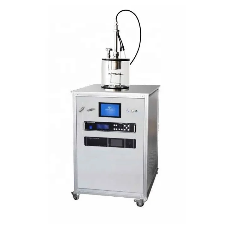
Rf sputtering system. The Glow Research SputterGlow is a flexible sputter deposition system designed to process 0mm wafers, 156mm x 156mm solar cells or smaller wafers–including pieces of wafers The SputterGlow can have up to three interchangeable process stations (each station can be configured for heating, sputter deposition or sputter etching). The system is rf magnetron sputtering with has a automatic matching network The plasma is pinkish purple I have done this for 1hr still there is no silicon deposited on glass substrate. The system is rf magnetron sputtering with has a automatic matching network The plasma is pinkish purple I have done this for 1hr still there is no silicon deposited on glass substrate.
The system has an insitu Pt heater, which can produce substrate temperatures up to 400 ºC during deposition The system reaches an ultrahigh vacuum level of 3×10⁸ Torr The system design allows for both DC and RF sputtering as well as the cosputtering of multiple targets at once MultiFTS. Semiautomated processing of up to six 150mm or four 0mm substrates per run;. • RF sputtering has a wider range of application and is suitable for all the materials for conductive and nonconductive materials, but it most commonly used for depositing of dielectric sputtering target materials • The deposition rate is lower compare with DC sputtering • It is used for smaller substrate sizes due to the high cost.
The Sputtering System used is in our lab for deposition of metals and ITO films is a 6" Perkin Elmer Model 2400 This is the oldest model of all the sputtering equipment in our labs current However, it is still capable of high quality uniform films as confirmed by AFM characterization. RF & DC Sputtering System Scientific & Analytical Instruments offers standard and customized RF/DC Magnetron Sputtering System in different size as per customer requirement to produce quality, thin and homogenous film coatings SAI Sputtering systems are versatile for thin film coatings in Research, Educational Institutions, Semiconductor. A sputter etch process will always require more RF power than an RF bias (only) process The substrate stage and its components will need to withstand the higher RF power and current flow – resulting in higher heating of the stage’s components.
A sputtering system is a machine in which a sputtering process occurs It contains the entire process and allows a user to adjust the temperature, power, pressure, target, and substrate materials Man with a drill. Features of Euclid's RF sputtering system “Turmeric” mobile workstation on wheels;. 300 Watt CW RF input power;.
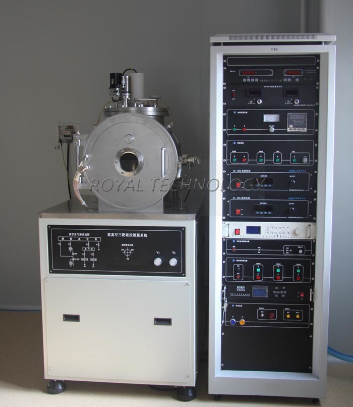
UHV environment down to the low 1010 Torr level ;. The new batch inline sputtering system from TFE provides DC magnetron, RF magnetron and RF diode capabilities in all sputtering positions, without changing the cathode RF etch capability is also included System operation is under PLC control (Mitsubishi model) A wide variety of options add to system’s flexibility and include PULSED power. UHV environment down to the low 1010 Torr level ;.
Sputtering Process Sputtering Deposition Method In terms of physics, Sputtering is a phenomenon in which energetic particles of plasma or gas hit the surface of a solid and microscopic particles are separated from it This phenomenon occurs naturally in outer space and can cause unwanted surface wear in high precision conditions. Sputter deposition is a physical vapor deposition (PVD) method of thin film deposited by sputtering The general sputtering method can be used to prepare a variety of materials such as metals, semiconductors, insulators, etc, and has the advantages of simple equipment, easy control, large coating area, and strong adhesion, and the magnetron sputtering method developed in the 1970s achieves. Plasmionique’s proprietary MAGNION Series sputtering cathodes are designed for high target utilization efficiency, and are available in balanced and unbalanced magnetic configurations in circular or rectangular shapes The magnetron cathodes are able to operate in DC, pulseDC, AC or RF biasing modes.
Being one of the trusted firms in the industry, we are highly engaged in providing a unique range of RF Magnetron Sputtering SystemOur products are known for better service lives and we are providing a full line of sputtering targets with various components from industrial grade to super high purity. Denton Vacuum Explorer 14 Sputtering System is used to deposit the thin films of dielectric material or metals by using magnetron gun Sputtering Definition Sputtering is a vacuum process in which a very thin film is deposited on substrates RF SPUTTER CONTROL Access to RF power supply, RF igniter, gas control, cathode selection, shutter. Sputtering Systems When materials matter most, your ultraprecise, highpurity, thin film layer devices will achieve maximum uniformity and repeatability with our on beam deposition systems SPECTORHT Ion Beam Sputtering System for Optical Coating.
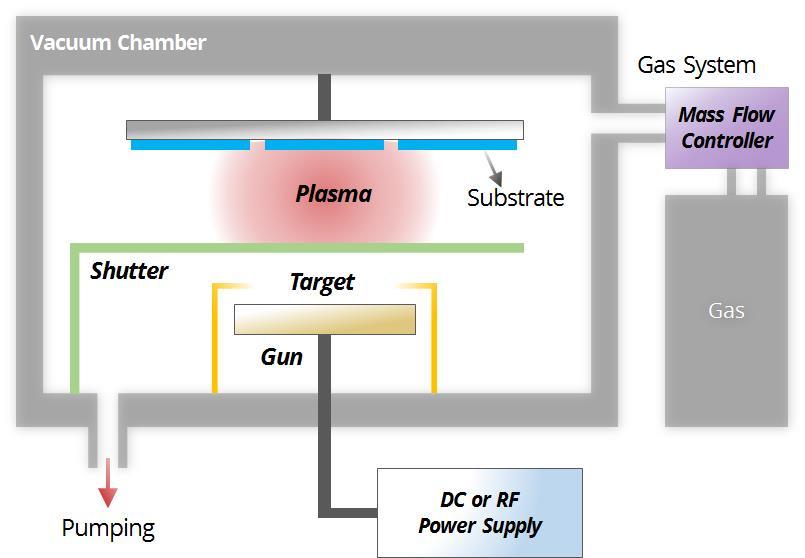
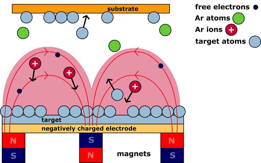
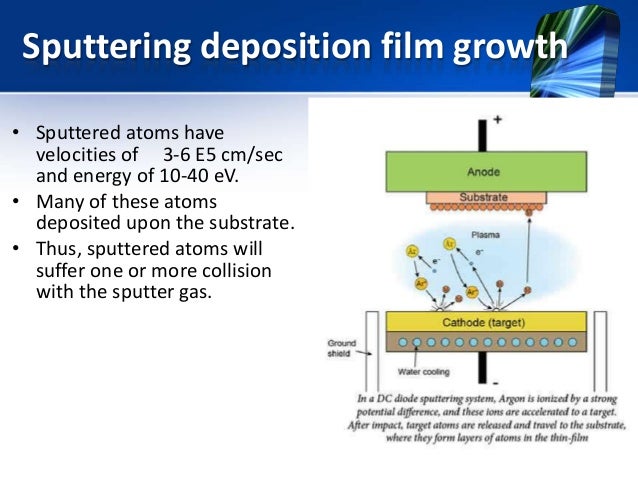
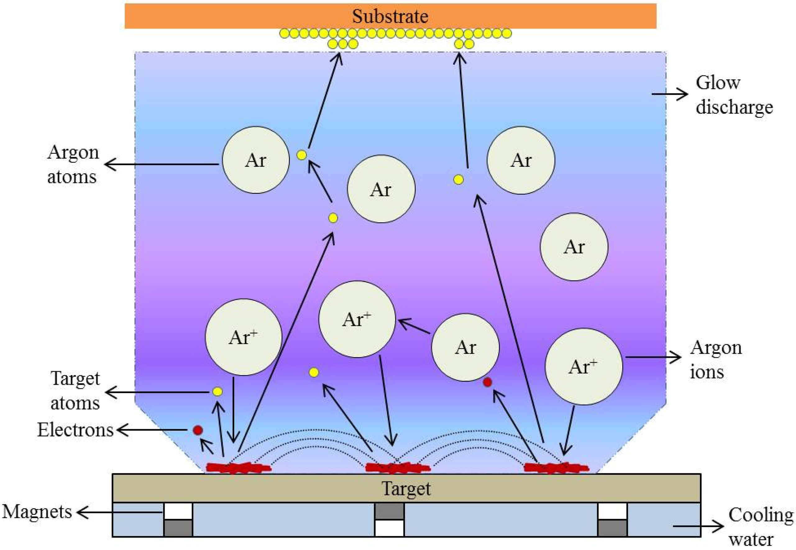
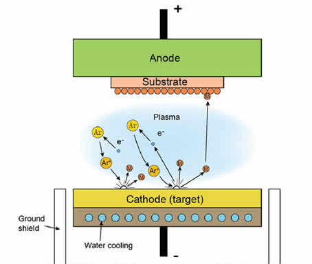
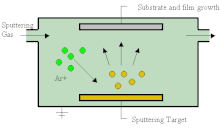
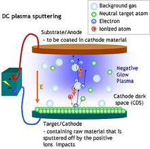
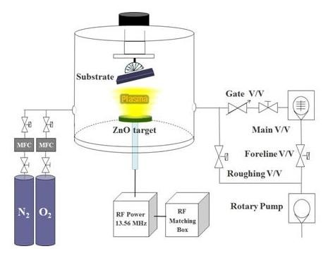
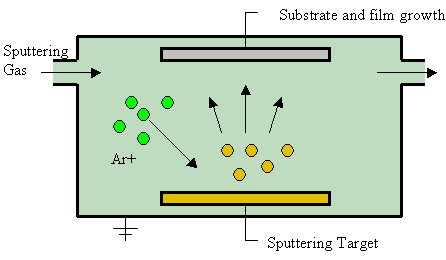
The system is rf magnetron sputtering with has a automatic matching network The plasma is pinkish purple I have done this for 1hr still there is no silicon deposited on glass substrate. These sputtering systems can be configured in either confocal, normal incidence, offaxis, glancing angle, or combination of target to substrate orientations Substrate holder features include radiant heating (1000°C), azimuthal rotation, RF/DC biasing, zmotion, cooling (H2O or LN2), tilting, or planetary motion. Sputtering Sputtering is a technology in which the material is released from the source at much lower temperature than evaporation The substrate is placed in a vacuum chamber with the source material, named a target, and an inert gas (such as argon) is introduced at low pressure.
HV or UHV RF/ DC/ Pulsed DC Compatible Magnetron Sputtering System Single as well as multi target sputter source option Sputter configuration available from 16 Sputter sources in sputter up or sputter down. 2480 RF Diode Batch System Productionproven 24/7 sputtering system;. The PerkinElmer of RF Plasma systems for sputtering and etching reflect an advanced design concept based on a high capacity load lock that permits wafer loading without breaking vacuum in the process chamber The Varian system sets the pace for stateoftheart wafer sputtering Check out our complete line.
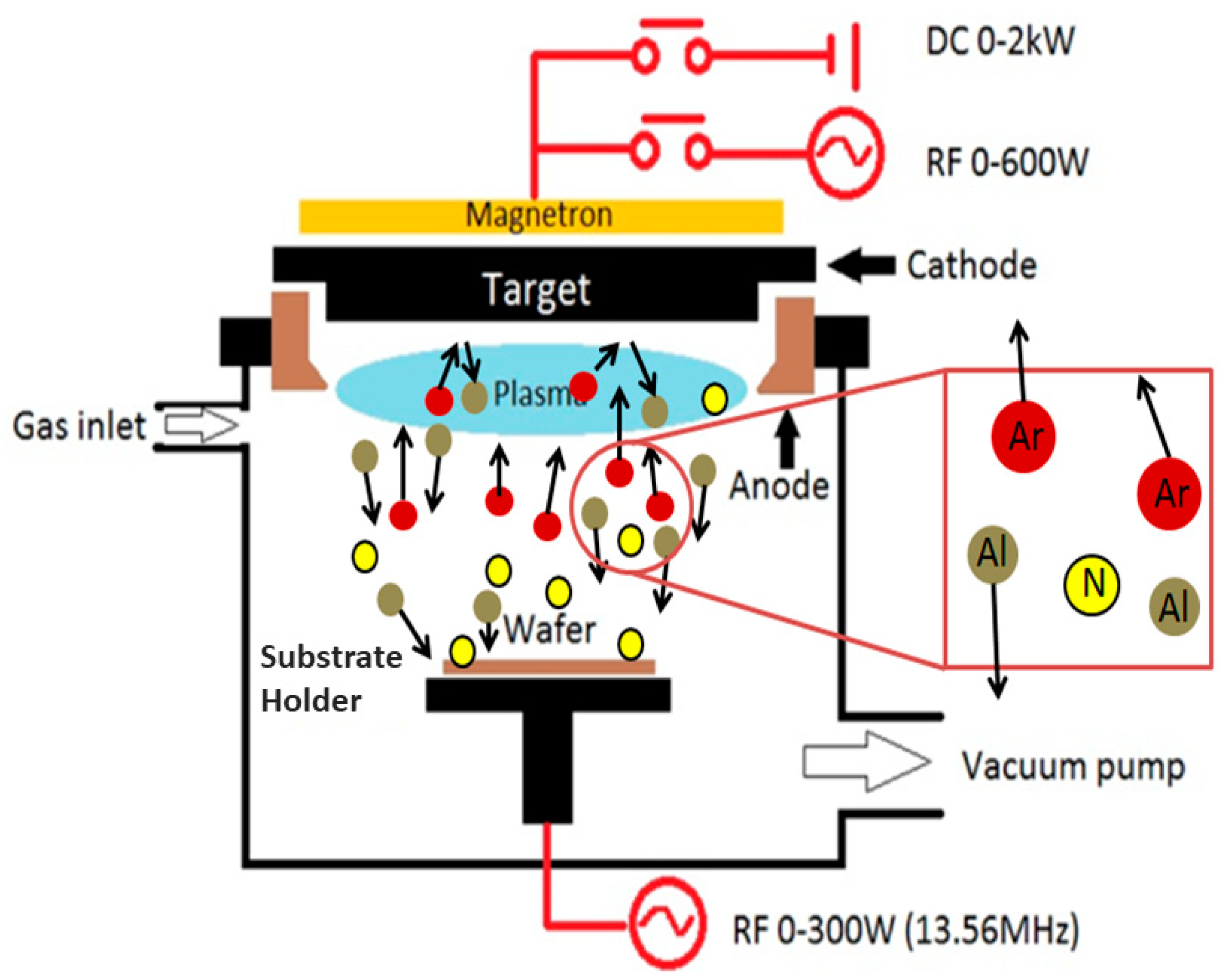
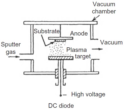
Denton Vacuum Explorer 14 Sputtering System is used to deposit the thin films of dielectric material or metals by using magnetron gun Sputtering Definition Sputtering is a vacuum process in which a very thin film is deposited on substrates RF SPUTTER CONTROL Access to RF power supply, RF igniter, gas control, cathode selection, shutter. This system is called RFdiode sputtering as shown in Fig 113 In the RFsputtering system, the thin films of the insulator are sputtered directly from the insulator target The deposition rates of sputtering systems are lower than those of vacuum deposition Lowering the sputtering pressure increases the deposition rates. It mentions RF sputtering advantages and RF sputtering disadvantages The figure1 below depicts RF sputtering system Silent features of the system are as follows • RF Source frequency 1356 MHz • RF peak to peak voltage 1000 V • Electron densities 10 9 to 10 11 Cm3 • Chamber pressure 05 to 10 mTorr There are two processes.
Sputtering is a process whereby particles are ejected from a solid target material due to bombardment of the target by energetic particles, particularly gas ions Sputtering is done either using DC voltage (DC sputtering) or using power delivered at Radio Frequency (RF sputtering) Other advanced sputtering process like Magnetron Sputtering, Reactive Gas Sputtering, Pulsed DC Sputtering etc. This system is called RFdiode sputtering as shown in Fig 113 In the RFsputtering system, the thin films of the insulator are sputtered directly from the insulator target The deposition rates of sputtering systems are lower than those of vacuum deposition Lowering the sputtering pressure increases the deposition rates. PRAXAIR MRC MRCGTI TI TITANIUM Sputtering Target Plate 45 SEMICORE / MRC SEC643 SC643 RF Sputter Coater Sputtering System 46 SiO2 sputtering target 4″ diameter 025″ thick sputter NEW old stock MRC 47 Sputtering Target Silicon Dioxide (SiO2) Diameter3 inch Thick05 inch4 pcs 48 TEL / MRC SPUTTER PART P/N A 49 TEL.
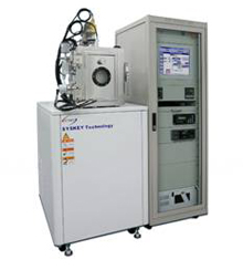
AJA Sputtering System AJA Sputtering System Located in VKNRC N122,the ATC00F sputtering system purchased from AJA International is a high performance and versatile system The system contains 4 magnetron sputtering guns (2 DC and 2 RF) which allow insitu tilting of their heads without breaking vacuum. Kurt J Lesker CMS18 sputter #4 (Reactive/Metals) Sputter Description The CMS18 is a flexible three target sputtering system with a load lock capable of small parts through 6” wafers The system is capable of depositing multilayer film stacks and alloys The system is also setup for substrate heating as well as RF biasing and sample pre. Features of Euclid's RF sputtering system “Turmeric” mobile workstation on wheels;.
RF substrate bias option to enhance deposited film properties;. RF Sputtering Instead of applying a DC voltage to the cathode, apply a voltage oscillating at radio frequency (RF), typically around 135 MHz The RF peak to peak voltage is around 1000V, electron densities are around 10 9. All stainless steel (from the gas cylinder regulator to the mass flow controller) UHP Argon supply system with purifier;.
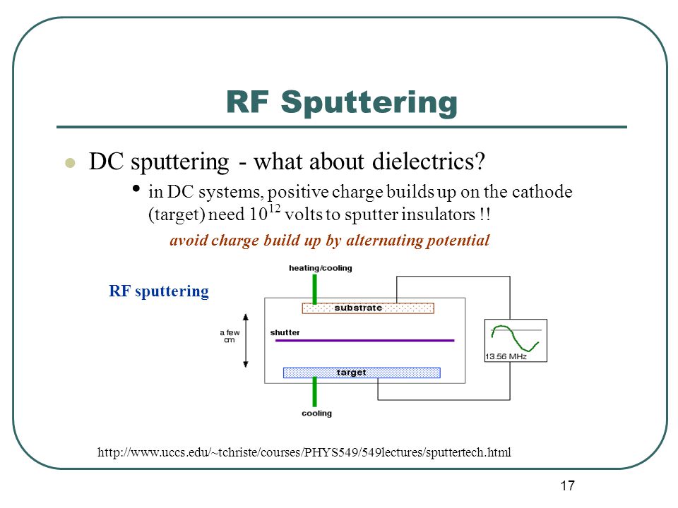
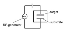
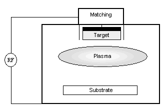
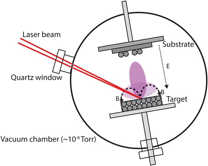
All metal sealings, custom cubical chamber, variable targettosubstrate distance by UHV actuator. Figure 1 RF Sputtering Configuration For RF sputtering, a highfrequency generator is used generating electromagnetic power in the MHzRegion (typical 1356 MHz) The output voltage and current capabilities of these generators are limited, so they need to work on a defined load impedance of 50 W. 300 Watt CW RF input power;.
300 Watt CW RF input power;. Figure 1 RF Sputtering Configuration For RF sputtering, a highfrequency generator is used generating electromagnetic power in the MHzRegion (typical 1356 MHz) The output voltage and current capabilities of these generators are limited, so they need to work on a defined load impedance of 50 W. The Sputtering System used is in our lab for deposition of metals and ITO films is a 6" Perkin Elmer Model 2400 This is the oldest model of all the sputtering equipment in our labs current However, it is still capable of high quality uniform films as confirmed by AFM characterization.
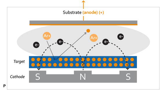
Being one of the trusted firms in the industry, we are highly engaged in providing a unique range of RF Magnetron Sputtering SystemOur products are known for better service lives and we are providing a full line of sputtering targets with various components from industrial grade to super high purity. The CMS18 is an extremely flexible three target reactive sputtering system with a load lock capable of small parts through 6" wafers It has 2 RF sources and one DC source with pulse functions The system is capable of depositing multilayer film stacks, alloys, and reactively sputtered oxides and nitrides. RF magnetron sputtering is a technique where Argon ions are accelerated by a RF electric field to hit a target made of the material to sputter The target is sputtered in all directions, in particular, sputtered atoms will reach the substrate placed in front of the target, but outside of the plasma, to prevent etching by the plasma.
Sputtering Systems NANOMASTER's state of the art Sputtering Systems can be constructed with various chamber and source configurations for depositing metals and dielectric thin films on to substrates up to 0 mm The systems can be equipped with DC, RF and Pulsed DC power supplies to enable sequential or cosputtering. KJLC ® TruPlasma Pulsed DC Sputtering Power Supplies KJLC offers a range of pulsed DC power options from 1kW 10kW These supplies can easily be integrated to any existing sputtering system and are ideal for optimal performance in reactive processes. This leads to drastically reduced sputter yields and deposition rates • The oxidation/nitridation is a runaway process Beyond a critical gas pressure, it progresses rapidly • Best oxide films are obtained just below this critical point • One solution is to oscillate the cathode voltage like RF sputtering but at a lower frequency (~100.
All metal sealings, custom cubical chamber, variable targettosubstrate distance by UHV actuator. Sputtering Process Sputtering Deposition Method In terms of physics, Sputtering is a phenomenon in which energetic particles of plasma or gas hit the surface of a solid and microscopic particles are separated from it This phenomenon occurs naturally in outer space and can cause unwanted surface wear in high precision conditions. All stainless steel (from the gas cylinder regulator to the mass flow controller) UHP Argon supply system with purifier;.
A sputter etch process will always require more RF power than an RF bias (only) process The substrate stage and its components will need to withstand the higher RF power and current flow – resulting in higher heating of the stage’s components. RF Sputter Deposition System The AJA Orion Sputtering System is a loadlocked sputtering system capable of depositing metal and dielectric films over a substrate up to 6 inches in diameter It is equipped with seven AJA high vacuum magnetron sputtering sources that are powered by two RF generators (300W) and three DC generators (750W) for. UHV environment down to the low 1010 Torr level ;.
DC Sputtering VS RF Sputtering What is Sputtering Sputtering is a vacuum deposition technique used to deposit thin film of a material onto a surface The substrates are placed into the vacuum chamber and pumped down to process pressure First, the creating gaseous plasma will accelerat e the ions from this plasma into some source material. All metal sealings, custom cubical chamber, variable targettosubstrate distance by UHV actuator. RF Sputter Deposition System The AJA Orion Sputtering System is a loadlocked sputtering system capable of depositing metal and dielectric films over a substrate up to 6 inches in diameter It is equipped with seven AJA high vacuum magnetron sputtering sources that are powered by two RF generators (300W) and three DC generators (750W) for.
HomeSolutionsSputtering Systems Sputtering is a process whereby particles are ejected from a solid target material due to bombardment of the target by energetic particles, particularly gas ions Sputtering is done either using DC voltage (DC sputtering) or using power delivered at Radio Frequency (RF sputtering). Cr coating was done by means of the RF sputtering technique from a metallic Chromium target of 9999 % purity using argon as a sputtering gas The deposition chamber was initially pumped to a base pressure of 80 × 10 −6 Torr and then back filled with Ar ( % purity) to a process pressure of 27 mT. PRAXAIR MRC MRCGTI TI TITANIUM Sputtering Target Plate 45 SEMICORE / MRC SEC643 SC643 RF Sputter Coater Sputtering System 46 SiO2 sputtering target 4″ diameter 025″ thick sputter NEW old stock MRC 47 Sputtering Target Silicon Dioxide (SiO2) Diameter3 inch Thick05 inch4 pcs 48 TEL / MRC SPUTTER PART P/N A 49 TEL.
Film thickness uniformities typically. Cosputtering multiple elements in a reactive process can produce complex ceramics An RF power supply is also present specifically for generating a localized plasma at the substrate This can be used as a surface cleaner, etcher, for techniques such as ionassisted deposition, and to assist in the reactive formation of metalnitrides. Features of Euclid's RF sputtering system “Turmeric” mobile workstation on wheels;.
It mentions RF sputtering advantages and RF sputtering disadvantages The figure1 below depicts RF sputtering system Silent features of the system are as follows • RF Source frequency 1356 MHz • RF peak to peak voltage 1000 V • Electron densities 10 9 to 10 11 Cm3 • Chamber pressure 05 to 10 mTorr There are two processes. This system is called RFdiode sputtering as shown in Fig 113 In the RFsputtering system, the thin films of the insulator are sputtered directly from the insulator target The deposition rates of sputtering systems are lower than those of vacuum deposition Lowering the sputtering pressure increases the deposition rates. All stainless steel (from the gas cylinder regulator to the mass flow controller) UHP Argon supply system with purifier;.
In square target with RF Diode sputter source;. Sputter deposition is a physical vapor deposition (PVD) method of thin film deposited by sputtering The general sputtering method can be used to prepare a variety of materials such as metals, semiconductors, insulators, etc, and has the advantages of simple equipment, easy control, large coating area, and strong adhesion, and the magnetron sputtering method developed in the 1970s achieves.

Rf Sputtering Principles Ifn Trento

Sputtering System Rf And Dc Sputtering Unit Importer From Bengaluru
Osa Optoelectronic Properties And Anisotropic Stress Of Mo Zno Thin Films Deposited On Flexible Substrates By Radio Frequency Magnetron Sputtering
Rf Sputtering System のギャラリー
3

A Schematic Diagram Of Rf Magnetron Sputtering System Download Scientific Diagram
Technical Research Centre Trc

Sputter Deposition An Overview Sciencedirect Topics
Magnetron Sputtering Deposition Systems Denton Vacuum
Sputtering Processes For Thin Film Deposition Ppt Video Online Download

Dc Rf Magnetron Sputtering System Samwon Vacuum Komachine

Radio Frequency Magnetron Sputter Deposition As A Tool For Surface Modification Of Medical Implants Intechopen
Rf Sputtering Advantages Rf Sputtering Disadvantages

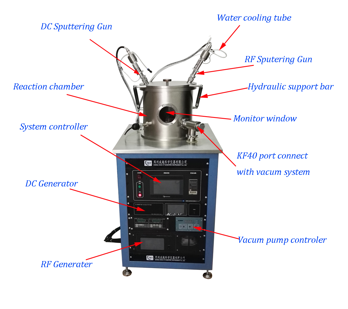
Lab Dc Rf Magnetron Sputtering Equipment System View Rf Sputtering Sputter System Cyky Product Details From Zhengzhou Cy Scientific Instrument Co Ltd On Alibaba Com

Rf Dc Magnetron Sputtering System Apt Advanced Process Technology
Sputtering System Aja Atc Orion 8 Polifab
Sputtering Process

Sciencecentral

What Is Dc Sputtering

Rf Sputtering Principles Ifn Trento

The Rf Sputtering System 19 Download Scientific Diagram
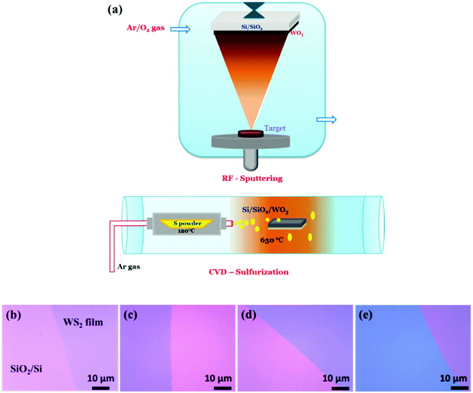
Layer Modulated Wafer Scale And Continuous Ultra Thin Ws2 Films Grown By Rf Sputtering Via Post Deposition Annealing Journal Of Materials Chemistry C Rsc Publishing
Coatings Free Full Text Recent Developments In R F Magnetron Sputtered Thin Films For Ph Sensing Applications An Overview Html

Radio Frequency Sputtering An Overview Sciencedirect Topics

Nano Point Nanotechnology Sputtering

Pulsed Dc Magnetron Sputtering Dc Sputtering Process Vaccoat

Sciencecentral

Faq Vaccoat

Development Of Rf Magnetron Sputtering Method To Fabricate Pzt Thin Film Actuator Sciencedirect
Q Tbn And9gcrs4t5gdkz1ormcnktha6w4d Cb6uby8bir Jwcoybrpe Zmzh8 Usqp Cau
Sputtering System Leybold Lh Z400 Polifab

Sputtering Thin Film Deposition Euclid Techlabs

Own Industrial Rf Dc Sputtering System Rs Piece S Scientific Analytical Instruments Id
Q Tbn And9gcrmgxpgzucw S3sp1bixoax2godwfl3pff9llex4tglrv55bg8c Usqp Cau

Hybrid Pvd Coater In Glove Box 2 Rf Sputtering 2 Evaporation Source Vtc H3 Gb
3 0 General Experimental Techniques Growth And Study Of Magnetostrictive Fesibc Thin Films For Device Applications

Rf Sputtering Manual 10 Pdf Date Of Creation Sabiha Sultana Seher Sabz Gmail Com Rf Magnetron Sputtering System Make Anelva Sputtering Unit Model Course Hero
Radio Frequency Magnetron Sputter Deposition As A Tool For Surface Modification Of Medical Implants Intechopen
Advances In Rf Sputtering Aultimut
Magnetron Sputtering Deposition Systems Denton Vacuum
Edwards Auto 306 Dc And Rf Sputter Coater Berkeley Microlab
Sputter Deposition Wikipedia

Indigenously Designed Locally Fabricated Rf Sputtering System Download Scientific Diagram

A Schematic Diagram Of Facing Target Rf Magnetron Sputt Open I

Edwards Auto 500 Turbo Three Target Rf Sputtering System Thin Film Deposition Semistar
Magnetron Plasma Sputtering Coater

Rf Sputtering Principles Ifn Trento
Sensors Free Full Text Reactive Sputtering Of Aluminum Nitride 002 Thin Films For Piezoelectric Applications A Review Html

A Schematic Diagram Of The Radiofrequency Rf Sputtering System For Download Scientific Diagram
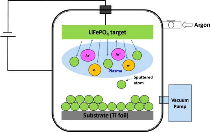
Sputtered Porous Li Fe P O Film Cathodes Prepared By Radio Frequency Sputtering For Li Ion Microbatteries Scientific Reports

Adnanotek Magnetron Sputtering Deposition Sputter System E Beam Evaporator Pld Pulsed Laser Deposition

Denton Vacuum Dv 602 Single Target Rf Sputtering System 21 Ebay

Sputtering Configurations A Dc Sputtering B Rf Sputtering Download Scientific Diagram

Rf Magnetron Sputtering System At Rs Piece Sputtering Systems Id

What Is Rf Sputtering
Scientific Analytical Instruments Rf Dc Sputtering System

Rf Magnetron Sputtering Ppt

China Pvd Magnetron Sputtering System Rf Dc Sputtering Deposition System For Laboratory China Magnetron Sputtering Machine Magnetron Sputter System

Magnetron Sputtering System Facility

Deposition Of Titanium Nitride Thin Films Onto Silicon By Rf Reactive Magnetron Sputtering Scientific Net

Sputtering Wikipedia

2 Rf Plasma Magnetron Sputtering Coater For Non Conductive Thin Films Vtc 2rf

Dc Rf Dual Head High Vacuum 2 Magnetron Plasma Sputtering Coater Vtc 600 2hd
Reactive Sputtering Deposition Presentation

China 3 Heads Compact Rf Plasma Magnetron Sputtering Deposition System China Rf Sputtering Deposition Systems Metal Substurates Magnetron Sputter Coater
Ppt Rf Magnetron Sputtering System Powerpoint Presentation Free Download Id

Dr Shabbir A Bashar S Ph D Thesis Chapter 3 Section 2

1 Schematic Drawing Of A Rf Sputtering System Adapted From 92 Download Scientific Diagram
Coatings Free Full Text Generation Of Charged Ti Nanoparticles And Their Deposition Behavior With A Substrate Bias During Rf Magnetron Sputtering Html
Q Tbn And9gcqrrma6pky5 U7sohjkjyiiokgbcikxhutol4ab7etg5jamztgg Usqp Cau

Sputtering

Research Center For Magnetic And Spintronic Materials

Influence Of The Substrate Bias Voltage On The Crystallographic Structure And Surface Composition Of Ti6a14v Thin Films Deposited By Rf Magnetron Sputtering
Advances In Rf Sputtering Aultimut
Coatings Free Full Text Rf Dc Magnetron Sputtering Deposition Of Thin Layers For Solar Cell Fabrication Html

Angstrom Engineering Dc Rf Sputtering System Centre For Integrated Rf Engineering University Of Waterloo
Faq Nanostructured Coatings Co
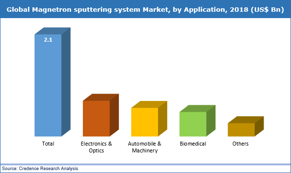
Magnetron Sputtering System Market Size Analysis Trends And Forecast To 27
Kurt J Lesker Company Combinatorial Magnetron Sputtering Advances With New Tools And New Predictive Techniques Vacuum Science Is Our Business
Structural And Optical Properties Of A Radio Frequency Magnetron Sputtered Zno Thin Film With Different Growth Angles Nanoscale Research Letters Full Text
Www Physlab Org Wp Content Uploads 16 04 Murtaza Presentaion Pdf

What Is Rf Sputtering
Kundoc Com Download Rf Sputtering Of Plastics 5a6b970fd64ab2dd0e Html
Dc Rf Magnetron Sputtering System Radio Frequency Pvd Deposition Coating Machine Buy Rf Mangeton Sputtering System Rf Magnetron Sputtering Coating Machine Dc Magnetron Sputtering System Product On Alibaba Com

Rf Sputtering Principles Ifn Trento
Lab Dc Rf Magnetron Sputtering Equipment System View Rf Sputtering Sputter System Cyky Product Details From Zhengzhou Cy Scientific Instrument Co Ltd On Alibaba Com

Iran Nanoelectronic Center Equipments
Scientific Analytical Instruments Rf Dc Sputtering System

Optimization Of Sputtering Parameters For The Deposition Of Low Resistivity Indium Tin Oxide Thin Films

Difference Between Rf Sputtering And Dc Sputtering Rf Sputtering Vs Dc Sputtering
Combined Magnetron Sputtering And Pulsed Laser Deposition Of Tio 2 And Bfco Thin Films Scientific Reports
Laboratory Dc And Rf Sputtering Coating Machine Dc Mf Sputtering Lab Coating Unit R D Lab Sputtering System
Www Physlab Org Wp Content Uploads 16 04 Murtaza Presentaion Pdf
Http Nano3 Calit2 Net Equipment Documents Op Procedure 48 Pdf
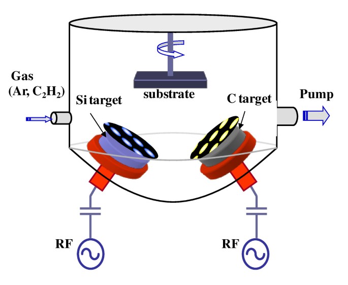
Sic Formation For A Solar Cell Passivation Layer Using An Rf Magnetron Co Sputtering System Nanoscale Research Letters Full Text
Rf Sputtering System With Tmp At Best Price In Noida Uttar Pradesh Vacuum Equipment Co

Sputtering Power Induced Physical Property Variation Of Nickel Oxide Films By Radio Frequency Magnetron Sputtering

1 Schematic Diagram Of Radio Frequency Rf Sputtering System From Download Scientific Diagram

Figure 2 From Characterization Of Thin Film Nickel Ni Deposition By Sputtering Method Semantic Scholar

Sputter Deposition An Overview Sciencedirect Topics

Faq Vaccoat

China New Designed Rf And Dc Power Supply Magnetron Sputtering System With Two Targets China Rf And Dc Power Supply Magnetron Sputtering Machine
Sputter Deposition Wikipedia
Large Area Continuous And High Electrical Performances Of Bilayer To Few Layers Mos 2 Fabricated By Rf Sputtering Via Post Deposition Annealing Method Scientific Reports

Schematic Of The Ito Rf Sputtering System Download Scientific Diagram


