
Rf Sputtering Pdf
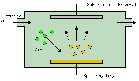
Sputtering process ablation of target P ≈ m Torr cathode anode ⊕ V ≈1kVEx v v e− Ar Cathode is “target”, source material cathode anode ⊕ V ≈1kVMostlyneutral source atoms (lots of e’s around) Target material (cathode) must be conductive or must use RF sputtering (later) Momentum transfer of Ar on cathode erodes.

Rf sputtering pdf. Using a combination process of rf sputtering and MHDPCVD Figure 1 illustrates the schematic diagram of an experimental setup sustaining two discharge plasmas in a deposition chamber The discharge plasma #1 was an rf sputtering for DLC film deposition, which was sustained with rf magnetron cathode with a 1 inch graphite target using a. HV or UHV RF/ DC/ Pulsed DC Compatible Magnetron Sputtering System Single as well as multi target sputter source option Sputter configuration available from 16 Sputter sources in sputter up or sputter down. RF powder sputtering t TO RF SUPPLY Figure 1 Block diagrams of the RF sputtering system with the important accessories a Conventional and b Modified (1target, 2cathode shield, 3plasma region, 4anode (substrate holder), 5argon gas inlet, 6RF tuning network, 7gasoutlet, 8coolant water) smaller by reducing the argon gas pressure.
Effect of RF Sputtering Process Parameters on Silicon Nitride Thin Film Deposition Sachin S Bharadwaj a, Shivaraj B Wa*, GR Rajkumara, M Krishna , aDepartment of Mechanical Engineering, R V College of Engineering, Bangalore, , India Abstract The objective of this work was to study the RF sputtering process parameters optimisation for deposition of Silicon Nitride thin. RF/DC Magnetron Sputtering System HV or UHV RF/ DC/ Pulsed DC Compatible Magnetron Sputtering System Single as well as multi target sputter source option;. RF Sputtering DC Pulsed power supplies are much less expensive than RF generators and matching networks Deposition of dielectric films by RF sputtering requires expensive and fragile ceramic targets DC Pulsed reactive sputtering is performed with less metal targets RF sputtering of dielectrics does not require a reactive process control.
For rf, as with dc sputtering, the deposition rate may be uniquely related to the power delivered to the target electrode The power delivered to the electrode is less than the power delivered by the rf generator by an amount equal to the rf losses in the system These losses can be substantial and quite variable, even when a good match is indicated at the generator. In general sputtering or etching applications, power generators are used to transfer either DC, Medium Frequency (typically in the several kHz range) or RF (usually in the several MHz) power into a chamber where the sputtering or etching is to take place With steady state DC power (no oscillations), there is no need for impedance matching. Using a combination process of rf sputtering and MHDPCVD Figure 1 illustrates the schematic diagram of an experimental setup sustaining two discharge plasmas in a deposition chamber The discharge plasma #1 was an rf sputtering for DLC film deposition, which was sustained with rf magnetron cathode with a 1 inch graphite target using a.
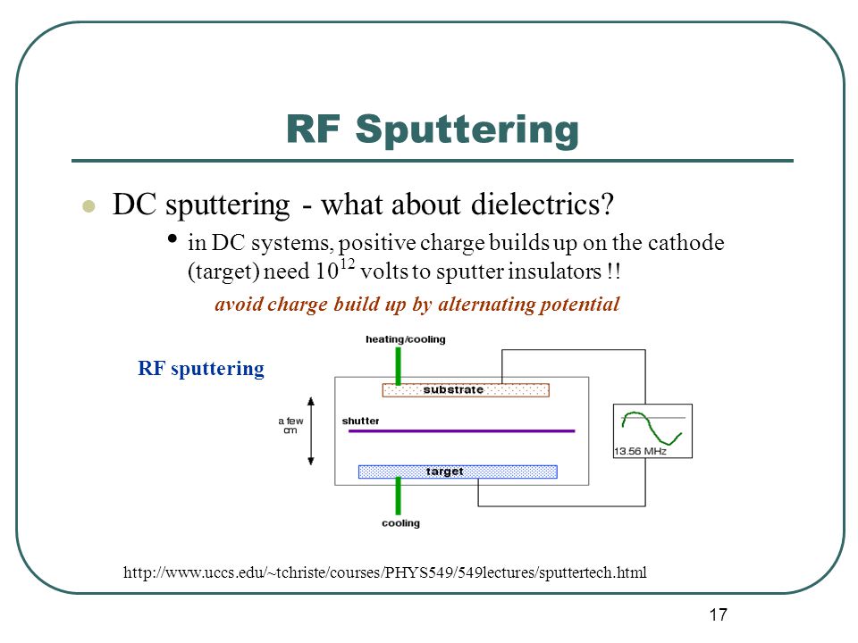
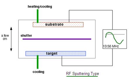
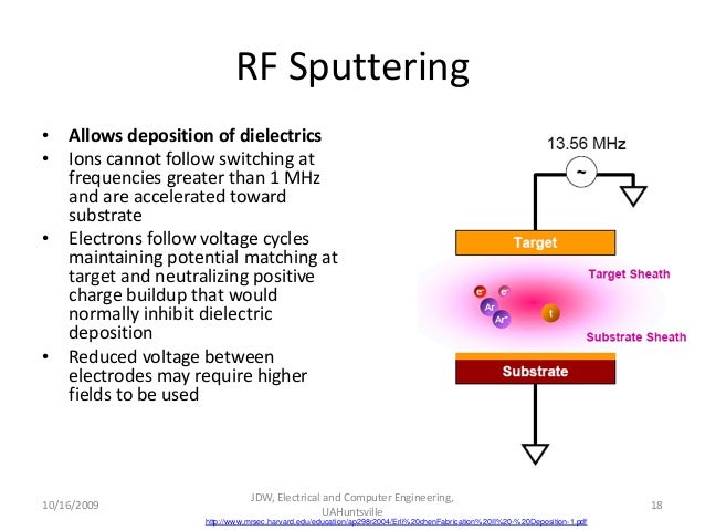
Rf sputtering can be used to sputter insulating material, although the sputtering rate is low A major disadvantage of rf sputtering of dielectric targets is that most insulating materials have poor thermal conductivity and high coefficients of thermal expansion, and are usually brittle materials Since most of the. RF (Radio Frequency) Sputtering DC sputtering cannot be used for depositing dielectrics because insulating cathode will cause charge build up during Ar bombarding ¨reduce the voltage between electrodes ¨discharge distinguishes Substrate 1356 MHz eAr eAr t Target Target Sheath Substrate Sheath ~ Solution use AC power. Rf sputtering can be used to sputter insulating material, although the sputtering rate is low A major disadvantage of rf sputtering of dielectric targets is that most insulating materials have poor thermal conductivity and high coefficients of thermal expansion, and are usually brittle materials Since most of the.
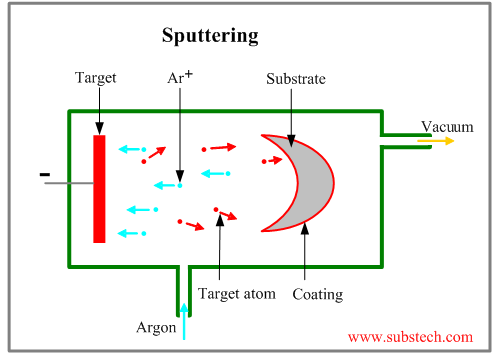
To obtain a suitable ohmic contact with the lowest resistivity, chromium (Cr) thin films were deposited on transparent conductive oxide indium tin oxide (ITO) by RF sputtering method in argon atmosphere and its electrical properties were optimized The deposition of Cr thin film has been performed for the layers with thickness of 150, 300 and 600 nm in constant Ar gas flow of 30 SCCM. Or DC sputtering ionbeam sputtering, reactive sput tering but all these are variants of the same physi cal phenomenon Sputtering is the process whereby atoms or molecules of a material are ejected from a target by the bombardment of highenergy particles More significantly cathodic sputtering is the process. Rf sputtering can be used with a magnetic field in balanced and unbalanced configurations to obtain a result similar to dclike diode discharge In fig 2 the different configurations of dc.
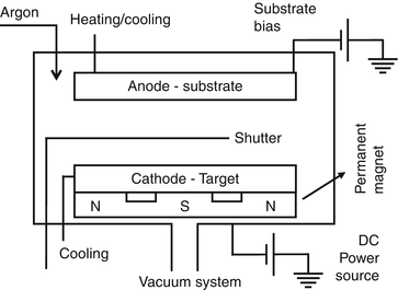
And during the sputtering process, the system is equipped with pressure gauges (also not shown) Sputter sources and substrate heater A sputtering system may be equipped with DC or RF sputtering sources, which have to be connected to the appropriate power supply A sputtering source consists of a cathode – target assembly, preferably with a magnetron The cross section shown in Fig 336. This leads to drastically reduced sputter yields and deposition rates • The oxidation/nitridation is a runaway process Beyond a critical gas pressure, it progresses rapidly • Best oxide films are obtained just below this critical point • One solution is to oscillate the cathode voltage like RF sputtering but at a lower frequency (~100. 1 Sputter deposition processes D Depla 1, S Mahieu 1, JE Greene 2 1 Ghent University, Department of Solid State Sciences, Krijgslaan 281 (S1), 9000 Ghent, Belgium 2 Materials Science and Physics Departments and the Frederick Seitz Materials Research Laboratory, University of Illinois, Urbana, Illinois , USA Sputter deposition is a widely used technique to deposit thin films on substrates.
Effect of RF Sputtering Process Parameters on Silicon Nitride Thin Film Deposition Sachin S Bharadwaj a, Shivaraj B Wa*, GR Rajkumara, M Krishna , aDepartment of Mechanical Engineering, R V College of Engineering, Bangalore, , India Abstract The objective of this work was to study the RF sputtering process parameters optimisation for deposition of Silicon Nitride thin. Would you like to get the full Thesis from Shodh ganga along with citation details?. For rf, as with dc sputtering, the deposition rate may be uniquely related to the power delivered to the target electrode The power delivered to the electrode is less than the power delivered by the rf generator by an amount equal to the rf losses in the system These losses can be substantial and quite variable, even when a good match is indicated at the generator.
Source—RF and DC sputtering, electron beam, ion beam, resis tance, and RF induction The Mark 50 is equipped with a unique, slidedown process chamber door at the front of the unit A builtin electronic rack assembly located alongside the chamber door contains all. Effect of RF Sputtering Process Parameters on Silicon Nitride Thin Film Deposition Sachin S Bharadwaj a, Shivaraj B Wa*, GR Rajkumara, M Krishna , aDepartment of Mechanical Engineering, R V College of Engineering, Bangalore, , India Abstract The objective of this work was to study the RF sputtering process parameters optimisation for deposition of Silicon Nitride thin. In the present work, we report low temperature (.
341 Sputtering (DC/RF/Reactive RF) Besides DC magnetron sputtering 16, RF magnetron sputtering 13 and reactive RF sputtering 32 are reported to be other efficient methods to synthesize uniform, stable, highly crystalline and stoichiometric films yielding reproducible and endurable RRAM devices In these processes, ion beam is bombarded. Typically, RF makes a better thin film than DC, pulsed DC, or AC The RFsputtered film will be smoother and have better packing density RF also deposits the film at about % of the DC rateIf you want to sputter using DC, pulsed DC, or AC, you must have a conductive (or semiconductive) target. Incorporated MAK sputter sources (13, 2, and 3, 4 and 6 inch) provide shielded electrical paths which allow RF as well as DC power to the cathode with minimum line losses and low reflection of RF power The MAK sputter source has a unique feature of allowing low operational pressures (05 millitorr).
Suitable for codeposition as well as sequential deposition;. Technical Specifications for the DC and RF sputtering unit 1 Magnetron cathode (2 nos) One to be connected to DC and the other to RF power supply • 2 “ Diameter with water cooling (indirect) arrangement • Stainless steel design and builtin shutter • SmCo magnet • 5 Amps maximum current • Bake out temperature 100 – 150 oC. RFsputtering is a suitable technique to fabricate optical planar waveguides and photonic microcavities operating in the visible and NIR regions Sputtering techniques are widely used in industrial process because high quality films can be obtained at low temperature substrates We have also demonstrated as the rf sputtering is a suitable.
RF sputtering A viable tool for MEMS fabrication 545 obtain highly caxis oriented films, which is a requirement for these films to be piezoelectric in nature In addition to the dielectric films, thin films of Cr, Au, Ti and Pt on silicon or glass substrates, (used for ZnO deposition) were also deposited by RF sputtering process. Procedure – RF Sputtering Using CVC 601 Tool 05/13/08 File Procedure – RF Sputtering Using CVC 601 Tool 12 Turn on RF power and adjust power level as necessary Typical power in 50 watts Maximum is 100 watts 13 Verify matching network controller is operating near the midrange on both tune and load 14. RF Sputtering DC Pulsed power supplies are much less expensive than RF generators and matching networks Deposition of dielectric films by RF sputtering requires expensive and fragile ceramic targets DC Pulsed reactive sputtering is performed with less metal targets RF sputtering of dielectrics does not require a reactive process control.
For RF sputtering, a highfrequency generator is used generating electromagnetic power in the MHzRegion (typical 1356 MHz) The output voltage and current capabilities of these generators are limited, so they need to work on a defined load impedance of 50 W. High quality indium tin oxide (ITO) thin films were grown without oxygen by both dc and RF magnetron sputtering techniques on glass substrates The effects of substrate temperature, film thickness and sputtering method on the structural, electrical and optical properties of the asgrown films were investigated. RF magnetron sputtering is a technique where Argon ions are accelerated by a RF electric field to hit a target made of the material to sputter The target is sputtered in all directions, in particular, sputtered atoms will reach the substrate placed in front of the target, but outside of the plasma, to prevent etching by the plasma.
This type of sputtering is known as “RF sputtering”, (figure 2) Page KFUPM 2 Figure 2 Basic elements of an RF sputtering system In order to increase the efficiency of the sputtering process, it is common for the sputtering source to have some magnetic confinement through a magnetron source The effect of the. Original Paper phys stat sol (b) 242, No 9, 17 – 11 (05) / DOI /pssb Growth of GaP1–xNx thin films by rf sputtering A PulzaraMora*, 1, 2, M MeléndezLira1, S JiménezSandoval3, and M LópezLópez1 1 Physics Department, Centro de Investigación y Estudios Avanzados del IPN, Apartado Postal , México DF, México 2 Departamento de Física y. 32 ITO Deposition by Reactive rf Sputtering The basic principles of reactive rf sputtering technique are described below This is followed by a discussion about the calibration of the system used in this work 321 Principles A sputtering system consists of an evacuated chamber, a target (cathode) and a substrate table (anode).
Abstract Chromium (Cr) films were deposited on plain carbon steel sheets by dc and rf magnetron sputtering as well as by electroplating Effects of dc or rf sputtering power on the deposition rate and properties such as, hardness, adhesion strength, surface roughness and corrosion resistance of the Cr films were investigated. This type of sputtering is known as “RF sputtering”, (figure 2) Page KFUPM 2 Figure 2 Basic elements of an RF sputtering system In order to increase the efficiency of the sputtering process, it is common for the sputtering source to have some magnetic confinement through a magnetron source The effect of the. Research RF Sputtering Packages Shown with 3" Polaris™ Adjustable Position Source with Tilt and Shutter 300 or 600 Watt Low Cost Packages for Those With Limited Budgets Desiring Full Capability 1356 MHz RF Power Generator Allows All Materials to be Sputtered Automatic and Manual Impedance Matching Networks Available.
To learn more, explore DC magnetron sputtering, RF magnetron sputtering, and pulsed DC sputtering (links below) Magnetron sputtering is available in a variety of source configurations and compatible with many of Angstrom’s process control capabilities and advanced fixturing options. Difference between RF sputtering and DC sputtering RF sputtering vs DC sputtering This page compares RF sputtering vs DC sputtering and mentions difference between RF sputtering and DC sputtering What is Sputtering Sputtering is highly versatile vacuum coating system which is used for deposition of various coating materials Plasma gas is used ti knock atoms out of the target. Would you like to get the full Thesis from Shodh ganga along with citation details?.
For RF sputtering, a highfrequency generator is used generating electromagnetic power in the MHzRegion (typical 1356 MHz) The output voltage and current capabilities of these generators are limited, so they need to work on a defined load impedance of 50 W. In general sputtering or etching applications, power generators are used to transfer either DC, Medium Frequency (typically in the several kHz range) or RF (usually in the several MHz) power into a chamber where the sputtering or etching is to take place With steady state DC power (no oscillations), there is no need for impedance matching. Or DC sputtering ionbeam sputtering, reactive sput tering but all these are variants of the same physi cal phenomenon Sputtering is the process whereby atoms or molecules of a material are ejected from a target by the bombardment of highenergy particles More significantly cathodic sputtering is the process.
In the present work, the stress evaluation of RF sputtered silicon dioxide films for MEMS applications has been reported The films were deposited in argon atmosphere in the pressure range 5 mtorr at 300 W RF power using a 3 inch diameter silicon dioxide target The stress measurements were carried out using wafer curvature technique All the deposited films show compressive stress except. Homebuilt sputter is a fully automated PLC controlled deposition system All vacuum functionality and RF to DC switching is controlled by a programmable logic controller (PLC) from the system touchscreen The system features topdown sputtering so no clips or sample retention mechanism is required. The films were prepared by RF diode sputtering using a 3 inch diameter SiO2 target in argon atmosphere in the pressure range 5– mTorr and RF power from 100 to 300 W.
The sputtering method has been widely used in the SOFCs technology for YSZ 2,3 or GDC thin film depositions4,5 In this report, the results about the deposition by RF magnetron sputtering of 1÷3 µm GDC films on the anode substrates will be presented The GDC targets were fabricated using commercial or inhouse prepared powders. Rf sputtering can be used to sputter insulating material, although the sputtering rate is low A major disadvantage of rf sputtering of dielectric targets is that most insulating materials have poor thermal conductivity and high coefficients of thermal expansion, and are usually brittle materials Since most of the. Magnetron sputtering coating is a vacuum coating process that falls under the category of physical vapor deposition (PVD) and is mainly used for depositing metals, alloys, and compound textiles, and other material with a thickness up to 5μ In textile coatings, it is used to coat textile fabrics with metals to provide antimicrobial, antistatic, and electroconductive properties.
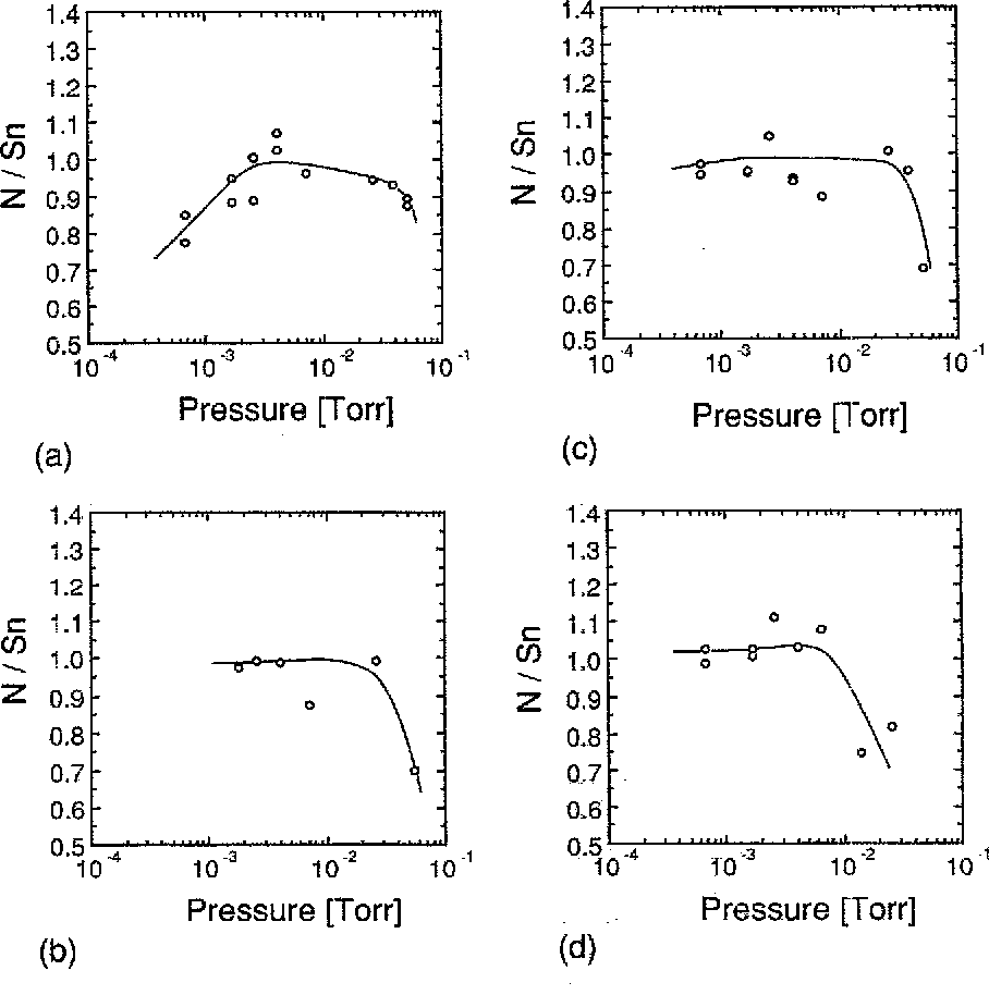
Sputtering process ablation of target P ≈ m Torr cathode anode ⊕ V ≈1kVEx v v e− Ar Cathode is “target”, source material cathode anode ⊕ V ≈1kVMostlyneutral source atoms (lots of e’s around) Target material (cathode) must be conductive or must use RF sputtering (later) Momentum transfer of Ar on cathode erodes. This leads to drastically reduced sputter yields and deposition rates • The oxidation/nitridation is a runaway process Beyond a critical gas pressure, it progresses rapidly • Best oxide films are obtained just below this critical point • One solution is to oscillate the cathode voltage like RF sputtering but at a lower frequency (~100. When sputtering Aluminum and Copper alloys, the film on the wafer has more copper than the target Reason At the target, the argon has achieved high enough energy to sputter the Al and Cu evenly However, in the gas (lower electric field), the heavier atoms are less effected by light sputter gas The light Al can gain enough energy to be.
The films were prepared by RF diode sputtering using a 3 inch diameter SiO2 target in argon atmosphere in the pressure range 5– mTorr and RF power from 100 to 300 W. RF Sputtering offers several advantages depending upon your specific application RF plasmas tend to defuse throughout the entire chamber rather than concentrating around the cathode or target material as with DC Sputtering RF Sputtering can sustain a plasma throughout the chamber at a lower pressure (115 mTorr). Difference between RF sputtering and DC sputtering RF sputtering vs DC sputtering This page compares RF sputtering vs DC sputtering and mentions difference between RF sputtering and DC sputtering What is Sputtering Sputtering is highly versatile vacuum coating system which is used for deposition of various coating materials Plasma gas is used ti knock atoms out of the target.
Sputter configuration available from 16 Sputter sources in sputter up or sputter down;.
Pdf Optical And Compositional Characterization Of Gaas Ti Thin Films Deposited By R F Magnetron Sputtering S Silvestre Academia Edu

What Is Rf Sputtering
Pdf Tin Nitride Thin Films Prepared By Radio Frequency Reactive Sputtering Semantic Scholar
Rf Sputtering Pdf のギャラリー
Nanopdf Com Download Nanometerthin Film Pdf
Sputtering Processes For Thin Film Deposition Ppt Video Online Download
Www Mdpi Com 1996 1944 11 3 439 Pdf

Rf Sputtering Principles Ifn Trento
Rf Sputtering Advantages Rf Sputtering Disadvantages
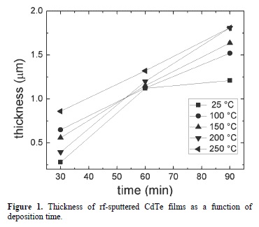
Effects Of Temperature And Deposition Time On The Rf Sputtered Cdte Films Preparation

What Is Dc Sputtering

Effects Of Temperature And Deposition Time On The Rf Sputtered Cdte Films Preparation
Nanopdf Com Download Nanometerthin Film Pdf
Pdf Nanostructural Features And Optical Performance Of Rf Magnetron Sputtered Zno Thin Films Praveen Tanwar Academia Edu

Development Of Rf Magnetron Sputtering Method To Fabricate Pzt Thin Film Actuator Sciencedirect

Top Pdf Rf Sputtering 1library
2

Structure Functional Property Relationships In Rf Sputtered Vanadium Dioxide Thin Films Journal Of Applied Physics Vol 102 No 11
Core Ac Uk Download Pdf Pdf
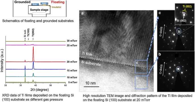
Preparation Of Highly 002 Oriented Ti Films On A Floating Si 100 Substrate By Rf Magnetron Sputtering Springerlink
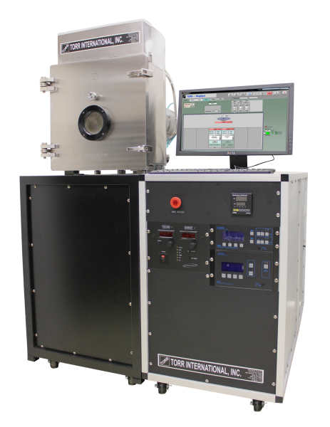
Magnetron Sputtering System Torr Internationalservices Llc
Layer Modulated Wafer Scale And Continuous Ultra Thin Ws2 Films Grown By Rf Sputtering Via Post Deposition Annealing Journal Of Materials Chemistry C Rsc Publishing
Www Physlab Org Wp Content Uploads 16 04 Murtaza Presentaion Pdf
Sputter Deposition Wikipedia
Sputter Deposition Wikipedia
Deep Uv Hexagonal Boron Nitride Hbn Baln Distributed Bragg Reflectors Fabricated By Rf Sputtering

Sputter Deposition An Overview Sciencedirect Topics

Top Pdf N Sub 2 Reactive Rf Sputtering 1library

Rf Magnetron Sputtered Coatings Deposited From Biphasic Calcium Phosphate Targets For Biomedical Implant Applications Sciencedirect

Pdf Silicon Nitride Thin Films By Rf Sputtering Application On Solid State Lithium Batteries
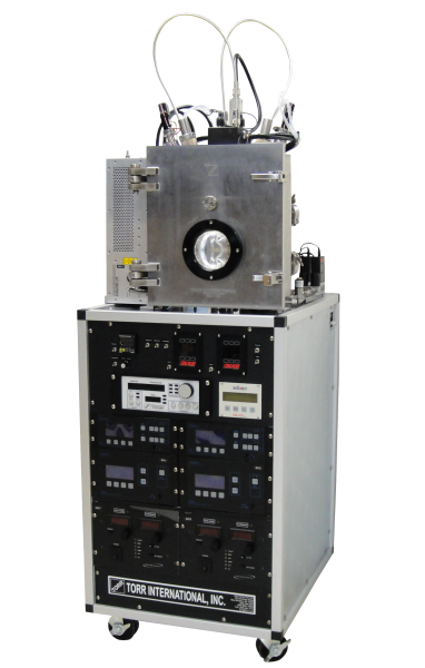
Magnetron Sputtering System Torr Internationalservices Llc
Part 6 Thin Film Depositoin
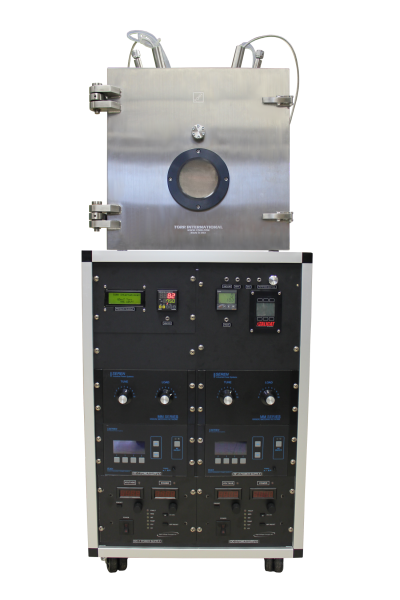
Magnetron Sputtering System Torr Internationalservices Llc
Sputtering Substech

Top Pdf N Sub 2 Reactive Rf Sputtering 1library
Cathode Sputtering Springerlink

Pdf Rf Sputtering A Viable Tool For Mems Fabrication

Electrical Properties Of Cualte2 Thin Films And Mocualte2 Contact Prepared By Rf Sputtering Pdf Document
Sputter Deposition Wikipedia

Pdf Main Properties Of Al2o3 Thin Films Deposited By Magnetron Sputtering Of An Al2o3 Ceramic Target At Different Radio Frequency Power And Argon Pressure And Their Passivation Effect On P Type C Si Wafers

Pdf Optimized Scratch Adhesion For Tisin Coatings Deposited By A Combination Of Dc And Rf Sputtering Masjuki Haji Hassan Academia Edu

Rf Sputtering Principles Ifn Trento

Top Pdf Rf Magnetron Sputtering Technique 1library

What Is Thin Film Deposition

Pdf Influence Of Sputtering Power On Properties Of Titanium Thin Films Deposited By Rf Magnetron Sputtering
Http Www Phys Sinica Edu Tw Tigp Nano Course 14 Spring Classnote Nanometer Thin film Pdf
Pdf Tin Nitride Thin Films Prepared By Radio Frequency Reactive Sputtering Semantic Scholar
Figure 1 From Degradation And Characterisation Of Resorbable Phosphate Based Glass Thin Film Coatings Applied By Rf Magnetron Sputtering Semantic Scholar

Pdf Main Properties Of Al2o3 Thin Films Deposited By Magnetron Sputtering Of An Al2o3 Ceramic Target At Different Radio Frequency Power And Argon Pressure And Their Passivation Effect On P Type C Si Wafers

Deposition Of Titanium Nitride Thin Films Onto Silicon By Rf Reactive Magnetron Sputtering Scientific Net
Q Tbn And9gcshlif7nuxioujxgd7nrra9kid5wmlqnopfe1n0rszeenv6uenq Usqp Cau
Q Tbn And9gcqrrma6pky5 U7sohjkjyiiokgbcikxhutol4ab7etg5jamztgg Usqp Cau
Http Www Mdpi Com 79 6412 4 4 756 Pdf
Materials Free Full Text Application Specific Oxide Based And Metal Dielectric Thin Film Materials Prepared By Radio Frequency Magnetron Sputtering Html

Sno2 Thin Films For Gas Sensor Prepared By R F Reactive Sputtering Pdf Document
Growth And Properties Of Zno Nanorods By Rf Sputtering For Detection Of Toxic Gases Rsc Advances Rsc Publishing
Http Staff Ustc Edu Cn Fuzp Course Paper Magnetron sputtering A review of recent developments Pdf
An Analysis Of Rf Sputtering Power And Argon Gas Pressure Affecting O

Composition Structure And Electrical Resistivity Of Zno1 X Films Deposited By Rf Magnetron Sputtering Under Various O2 Ar Gas Ratios Scientific Net

Influence Of The Substrate Bias Voltage On The Crystallographic Structure And Surface Composition Of Ti6a14v Thin Films Deposited By Rf Magnetron Sputtering

Pdf Synthesis Of Titanium Nitride Film By Rf Sputtering
Http Www Phys Sinica Edu Tw Tigp Nano Course 14 Spring Classnote Nanometer Thin film Pdf

D C Properties Of Zno Thin Films Prepared By R F Magnetron Sputtering Pdf Document

Self Organizing Plasma Behavior In Rf Magnetron Sputtering Discharges Journal Of Applied Physics Vol 125 No
Ultrathin Sputter Deposited Plasmonic Silver Nanostructures Nanoscale Advances Rsc Publishing Doi 10 1039 C9nah

The Effects Of Xe On An Rf Plasma And Growth Of Zno films By Rf Sputtering Pdf Zinc Oxide Thin Film

Tailoring Of Tio2 Film Microstructure By Pulsed Dc And Rf Magnetron Co Sputtering Sciencedirect
Reactive Rf Sputtering Of Vo2
D C Sputtering Springerlink
Q Tbn And9gcsmv5sez6h2h0cqzl7jqe7m54c0p2spndvowf Wnheskv3v Wsg Usqp Cau
Pdf Preparation By Rf Sputtering And P Type Conducting Transparent Characteristics Of Delafossite Mg Doped Cucro2 Thin Films Philippe Tailhades Academia Edu
Pdf Structural And Transport Properties Of Ndnio3 Thin Films Made By Rf Sputtering R Jardim And Marcia Escote Academia Edu

Top Pdf Rf Sputtering 1library
Archimer Ifremer Fr Doc Pdf
Hollow Metal Target Magnetron Sputter Type Radio Frequency Ion Source Pdf Download Free

Rf Sputtering Manual 10 Thin Film Sputtering

Magnetron Sputtering An Overview Sciencedirect Topics

Coatings Free Full Text Rf Magnetron Sputtering Deposition Of Tio2 Thin Films In A Small Continuous Oxygen Flow Rate

Nb3sn Thin Films Made By Rf Magnetron Sputtering Process With A Reacted Nb3sn Powder Target Pdf Document

Pdf The Effects Of Rf Sputtering Power And Gas Pressure On Structural And Electrical Properties Of Itio Thin Film
Structural And Electrical Properties Of Zno Prepared By Rf Sputtering Technique Thaksin University Journal
Q Tbn And9gcqqhtzcfsqsy7i2mpsmlenhngdm25 C4ebnn8hxlptkds26swjb Usqp Cau
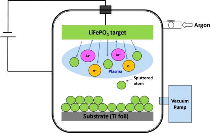
Sputtered Porous Li Fe P O Film Cathodes Prepared By Radio Frequency Sputtering For Li Ion Microbatteries Scientific Reports

Sputtering Configurations A Dc Sputtering B Rf Sputtering Download Scientific Diagram

Rf Sputtering Principles Ifn Trento

Impact Of Plasma Electron Flux On Plasma Damage Free Sputtering Of Ultrathin Tin Doped Indium Oxide Contact Layer On P Gan For Ingan Gan Light Emitting Diodes Son 18 Advanced Science Wiley Online

Sputtering Processes For Thin Film Deposition Ppt Video Online Download

What Is Rf Sputtering
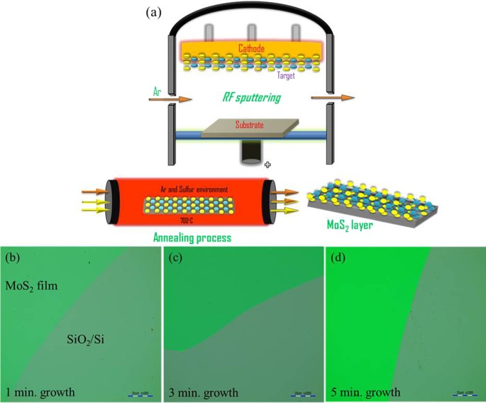
Large Area Continuous And High Electrical Performances Of Bilayer To Few Layers Mos 2 Fabricated By Rf Sputtering Via Post Deposition Annealing Method Scientific Reports
Pdf Deposition Of Bioactive Glass Ceramic Thin Films By Rf Magnetron Sputtering Joanny Fernandes Academia Edu

Sputter Deposition An Overview Sciencedirect Topics

Top Pdf Rf Magnetron Sputtering 1library

Top Pdf Rf Sputtering 1library
Pdf Properties Of Ito Films Deposited On Plastic Substrate By Rf Superimposed Dc Magnetron Sputtering Method
Pdf Nanostructured And Wide Bandgap Cds O Thin Films Grown By Reactive Rf Sputtering Dr Mohammad Aminul Islam Academia Edu
Nanopdf Com Download Nanometerthin Film Pdf
Osa Optical Properties And Residual Stress In Nb Si Composite Films Prepared By Magnetron Cosputtering
In Rich Alxin1 Grown By Rf Sputtering On Sapphire From Closely Packed Columnar To High Surface Quality Compact Layers Strathprints
Www Physlab Org Wp Content Uploads 16 04 Murtaza Presentaion Pdf

Rf Sputtering Manual 10 Thin Film Sputtering
Http Users Wfu Edu Ucerkb Nan242 L08 Sputtering B Pdf

Structural And Optical Changes Of Undoped Gan Layers Grown Via Radio Frequency Magnetron Sputtering Obtained From Gan Powders European Journal Of Engineering And Technology Research

Thin Film Evaporation Guide Film Evaporation Guide Pdfrf Rf Sputtering Is Effective Rf R Reactive Rf Thin Film Evaporation Guide Tasco Dc High Tantalum Solubility Gadolinium Pdf Document
Copper Deposition On Fabrics By Rf Plasma Sputtering For Medical Applications

Temperature Dependent Studies On Radio Frequency Sputtered Al Doped Zno Thin Film


