
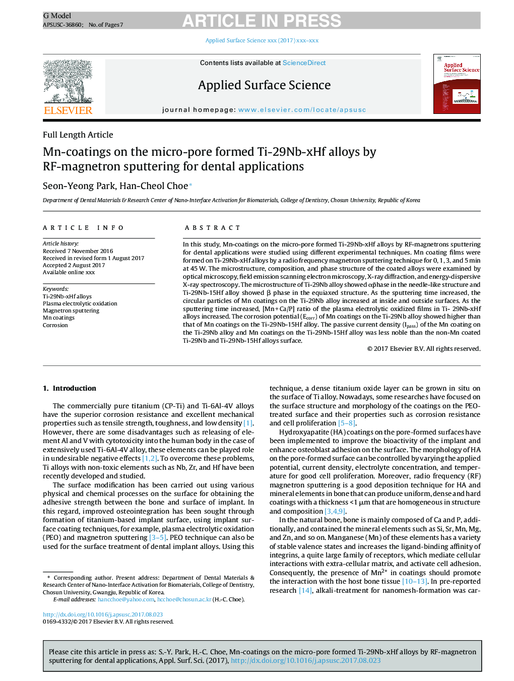
Rf Magnetron Sputtering
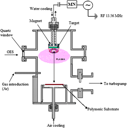
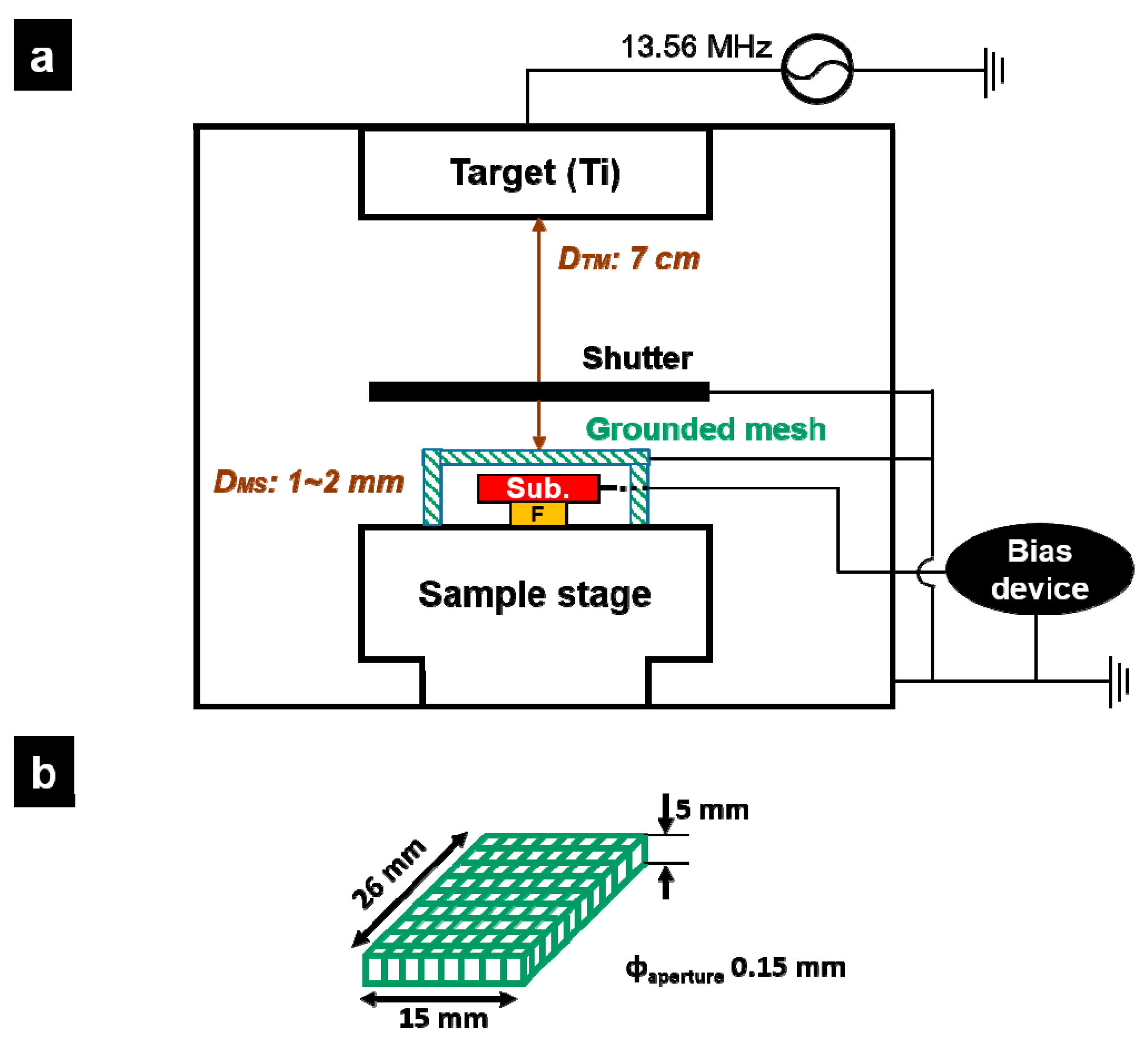
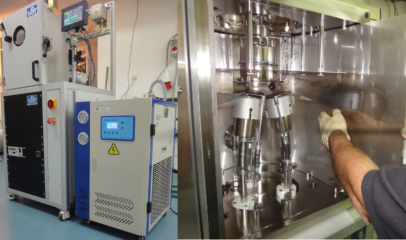
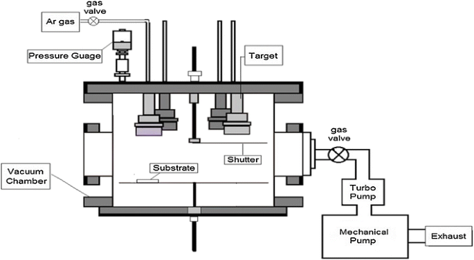
The depositions were performed with a RF magnetron sputtering PlasmalabSystem400 (Oxford Instruments, Abingdon, UK) using the parameters described in Table 1 The sputtering was made from a titanium target with a 150 mm diameter and 6 mm thickness, attached to a balanced magnetron.
Rf magnetron sputtering. An array of magnetron sputtering sources, using RF, DC, or pulsed DC power, are operated singly or in codeposition mode to produce a wide variety of film compositions. Both direct current (DC) and radio frequency (RF) power sources can be used with most magnetron cathodes Pulsed DC and low and mid frequency power supplies are also used in magnetron sputtering New concepts such as DC with RF overlay are also being developed for a number of coating applications (TCO’s for example). Three 7W DC power supplies units;.
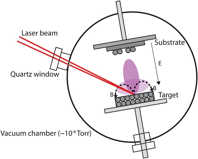
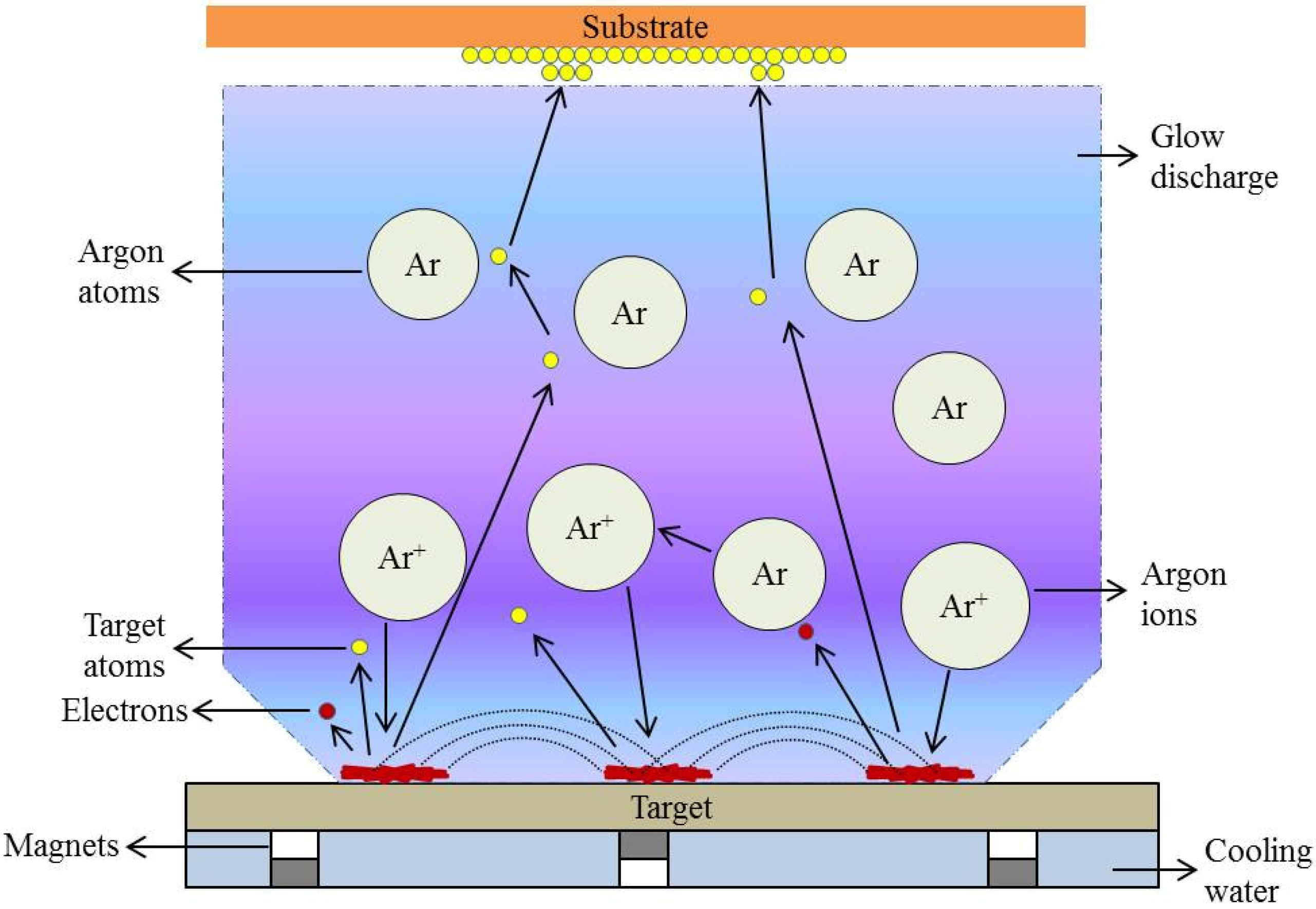
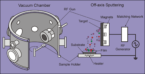
RF magnetron sputtering is a technique where Argon ions are accelerated by a RF electric field to hit a target made of the material to sputter The target is sputtered in all directions, in particular, sputtered atoms will reach the substrate placed in front of the target, but outside of the plasma, to prevent etching by the plasma. Magnetron sputtering is a highly versatile thin film deposition technique for coating films with excellent adhesion and high density A type of physical vapor deposition (PVD) coating technology, magnetron sputtering is a plasmabased coating process where a magnetically confined plasma is created near the surface of a target material. Abstract Molybdenum oxide (MoO 3) films were deposited on glass and silicon substrates held at temperature 473 K by RF magnetron sputtering of molybdenum target at various oxygen partial pressures in the range mbar The deposited MoO 3 films were characterized for their chemical composition, crystallographic structure, surface morphology, chemical binding configuration, and optical properties.
DOCUMENT HOMEBUILT RF & DC SPUTTER STANDARD OPERATING PROCEDURE Version 40 4 HARDWARE 21 3” magnetron gun, accepts 3” X 250” or 3” X 125” dielectric or nonmagnetic metal targets 22 300 Watt Seren RF sputtering supply 23 500 Watt MDX DC sputtering supply 24 N 2, Ar, & O 2 Process gases all using 50 SCCM MFC’s 25. Chitosanhydroxyapatite composite layers were deposited on Si substrates in radio frequency magnetron sputtering discharges The plasma parameters calculated from the currentvoltage radio frequencycompensated Langmuir probe characteristics indicate a huge difference between the electron temperature in the plasma and at the sample holder. RF & DC Sputtering System Scientific & Analytical Instruments offers standard and customized RF/DC Magnetron Sputtering System in different size as per customer requirement to produce quality, thin and homogenous film coatings SAI Sputtering systems are versatile for thin film coatings in Research, Educational Institutions, Semiconductor.
Another advantage of magnetron sputtering is the low process pressure (~ 5 x 10³ mbar) which increases the mean free path up to around mm As a result, the atomic particle stream of the target exhibits negligible scattering and retains its high output energy on the substrate, which results in forming very dense layers (fig right). HiPIMS DC pulsed power supply unit for dense film microstructures (1kW, 01kV, 0100A, max pulse rate 10 kHz) The pulsed source can be used by superimposing a DC bias voltage;. Http//wwwperkinelmersputtercom We have been focusing on providing solutions and enhancements to PerkinElmer Sputtering Systems including PerkinElmer P.
Maximum substrate size 4inch. As with DC Magnetron Sputtering, RF Magnetron sputtering coaters increases the growth of the thin film by increasing the percentage of target atoms which become ionized. RF and DC Magnetron Sputtering Unit Submitted by smpuricsr on Tue, 11 1448 RF and DC Magnetron Sputtering Unit Reference ME//033/RAMK/RF DC SPUTTER File Tender document Annexure 1 EMD CPP Proof Opening Date 01/12/ Closing Date 21/12/ Address.
Highpower impulse magnetron sputtering (HIPIMS or HiPIMS, also known as highpower pulsed magnetron sputtering, HPPMS) is a method for physical vapor deposition of thin films which is based on magnetron sputter depositionHIPIMS utilises extremely high power densities of the order of kW⋅cm −2 in short pulses (impulses) of tens of microseconds at low duty cycle (on/off time ratio) of < 10%. In reactive magnetron sputtering, titanium (Ti) is sputtered from a metallic target by energetic ions of a noble gas By supplying a reactive gas to the chamber, TiO 2 can be formed and deposited onto a chosen substrate. Magnetron sputtering is a highrate vacuum coat ing technique for depositing metals, alloys and compounds onto a wide range of materials with thicknesses up to about 5pm.
HV or UHV RF/ DC/ Pulsed DC Compatible Magnetron Sputtering System Single as well as multi target sputter source option Sputter configuration available from 16 Sputter sources in sputter up or sputter down. One 300W RF power supply unit with matching network;. RF/DC Magnetron Sputtering System HV or UHV RF/ DC/ Pulsed DC Compatible Magnetron Sputtering System Single as well as multi target sputter source option Sputter configuration available from 16 Sputter sources in sputter up or sputter down.
Radio frequency (RF) sputtering is a technique that is used to create thin films, such as those found in the computer and semiconductor industry Like direct current (DC) sputtering, this technique involves running an energetic wave through an inert gas to create positive ions. RF or Radio Frequency Sputtering is the technique involved in alternating the electrical potential of the current in the vacuum environment at radio frequencies to avoid a charge building up on certain types of sputtering target materials, which over time can result in arcing into the plasma that spews droplets creating quality control issues on the thin films – and can even lead to the complete cessation of the sputtering of atoms terminating the process. Magnetron Sputtering It was stated earlier (see Diode Sputtering) that DC diode sputtering has essentially fallen from use and has been superseded by DC magnetron sputtering For RF sputtering it is not quite as clearcut, there are some applications where RF diode sputtering is used in preference over RF magnetron.
Magnetron Sputtering in several configurations Single magnetron with rotating magnetic field, magnetron dia > substrate dia (see video) or Up to 4 magnetrons in confocal arrangement, magnetron dia < substrate dia (rotation required) or DRM 400 from Fraunhofer FEP with two concentric targets, magnetron dia > substrate dia. Pulsed magnetron sputtering The sputtering deposition of insulating materials poses some difficulties charging of the target and arcing, stoichiometry control and poisoning in reactive sputtering systems, low deposition rate and high costs for RF (Radio Frequency) sputtering. Radio frequency magnetron sputtering, also called RF magnetron sputtering is a process that is used to make thin film, especially when using materials that are nonconductive In this process, a thin film is grown on a substrate that is placed in a vacuum chamber.
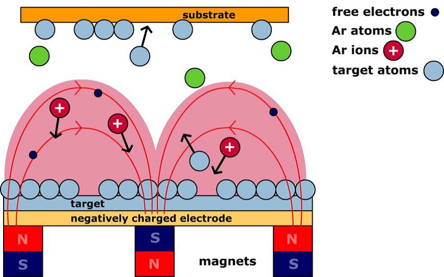
Magnetron sputtering is a highrate vacuum coat ing technique for depositing metals, alloys and compounds onto a wide range of materials with thicknesses up to about 5pm. Magnetron sputtering Thin film deposition by sputtering Permanent magnets increase the particle density One thing that all sputtering methods have in common is the heavy ion bombardment, usually using argon, which continuously removes material from the target surface which will condense on the substrate surface. Being one of the trusted firms in the industry, we are highly engaged in providing a unique range of RF Magnetron Sputtering SystemOur products are known for better service lives and we are providing a full line of sputtering targets with various components from industrial grade to super high purity.
High Power Impulse Magnetron Sputtering is a emerging process which uses a high current pulse to greatly increase the ionization of the sputtering material These ionized atoms have much higher energies than sputtered atoms in conventional magnetron sputtering and have been found to yield very dense and stable films. The aluminum oxide films were deposited in an RF magnetron sputtering coater equipped with an Omat cathode and Huettinger electronic PFG 5000 RF power supplies The cathode is configured with a planar annular permanent magnetic source. The main advantage of RF magnetron sputtering over DC magnetron sputtering is that it does not require the target as an electrode be electrically conductive Therefore, any material can be sputterdeposited theoretically using RF magnetron sputtering.
Both direct current (DC) and radio frequency (RF) power sources can be used with most magnetron cathodes Pulsed DC and low and mid frequency power supplies are also used in magnetron sputtering New concepts such as DC with RF overlay are also being developed for a number of coating applications (TCO’s for example). RF magnetron sputtering GdBa 2 Cu 3 O 7 − δ /La 067 Sr 033 MnO 3 quasibilayer films consists of two steps, which are the preparation of substrates and the RF magnetron sputtering process A picture of the sputtering system is shown in Figure S1. Four 3inch diameter magnetron sputter sources;.
Sputtering only occurs during negative bias This process is very amenable to reactive sputtering 4,5,6 Figure 2 Dual magnetron cathode configuration 1 Figure 3 Typical mid frequency power pulse 4 Pulsed magnetron sputtering overcomes two disadvantages of magnetron sputtering Loss (or hidden) of anode due to deposition of insulating. Abstract Chromium (Cr) films were deposited on plain carbon steel sheets by dc and rf magnetron sputtering as well as by electroplating Effects of dc or rf sputtering power on the deposition rate and properties such as, hardness, adhesion strength, surface roughness and corrosion resistance of the Cr films were investigated. RF sputtering can be used for metals, semiconducltors,, and insulators, and utilises RF power at a specific frequency of 1356 MHz, which has been allotted internationally for RF power supply.
Http//wwwperkinelmersputtercom We have been focusing on providing solutions and enhancements to PerkinElmer Sputtering Systems including PerkinElmer P. Dual magnetron sputtering uses a mid frequency (~ 40 kHz – 300 kHz) pulsed power source and two magnetron cathodes The dual magnetron configuration is shown in Figure 2, and a typical power pulse is shown in Figure 3. Abstract Molybdenum oxide (MoO 3) films were deposited on glass and silicon substrates held at temperature 473 K by RF magnetron sputtering of molybdenum target at various oxygen partial pressures in the range mbar The deposited MoO 3 films were characterized for their chemical composition, crystallographic structure, surface morphology, chemical binding configuration, and optical properties.
Both direct current (DC) and radio frequency (RF) power sources can be used with most magnetron cathodes Pulsed DC and low and mid frequency power supplies are also used in magnetron sputtering New concepts such as DC with RF overlay are also being developed for a number of coating applications (TCO’s for example). Magnetron Sputtering Systems PVD Products manufactures complete integrated sputtering systems to meet your specific deposition requirements These systems can be configured with multiple RF and/or DC magnetron sources ranging in size from 1 inch (25 mm) to 8 inches (0 mm) in diameter. Cuprous oxide (Cu2O) thin films were produced from metallic Cu targets on αAl2O3 (000l) substrate by radio frequency magnetron sputtering technology Three batches of samples were deposited under various sputtering parameters by modulating substrate temperature, gas flow and sputtering power, respectively The samples were characterized by Xray diffraction and fieldemission scanning.
• In RF sputtering, source of power is AC (Alternating Current) Instead of DC voltage to cathode, RF at about 135 MHz is being applied electron densities are 109to 1011Cm3and chamber pressure is 05 to 10 mTorr. Radio frequency (RF) sputtering is a technique that is used to create thin films, such as those found in the computer and semiconductor industry Like direct current (DC) sputtering, this technique involves running an energetic wave through an inert gas to create positive ions. RF (Radio Frequency) Sputtering DC sputtering cannot be used for depositing dielectrics because insulating cathode will cause charge build up during Ar bombarding ¨reduce the voltage between electrodes ¨discharge distinguishes Substrate 1356 MHz eAr eAr t Target Target Sheath Substrate Sheath ~ Solution use AC power.
Magnetron Sputtering It was stated earlier (see Diode Sputtering) that DC diode sputtering has essentially fallen from use and has been superseded by DC magnetron sputtering For RF sputtering it is not quite as clearcut, there are some applications where RF diode sputtering is used in preference over RF magnetron. The magnetron is the desing of highdepositionrare sputtering sources The magnetron is a magnetically assisted discharge As in the DC and RF sputtering arrangements there is a perpendicular (to the target surface) electric field. Being one of the trusted firms in the industry, we are highly engaged in providing a unique range of RF Magnetron Sputtering SystemOur products are known for better service lives and we are providing a full line of sputtering targets with various components from industrial grade to super high purity.
RF (Radio Frequency) Sputtering DC sputtering cannot be used for depositing dielectrics because insulating cathode will cause charge build up during Ar bombarding ¨reduce the voltage between electrodes ¨discharge distinguishes Substrate 1356 MHz eAr eAr t Target Target Sheath Substrate Sheath ~ Solution use AC power. PZT thin film was fabricated by using RFsputtering process, and platinum was used as bottom electrodes The sputtering gases were Ar:O2=25:0 sccm, Ar:O2=:5 sccm, or Ar:O2=15:10 sccm After sputtering, the PZT film was annealed for 5 minutes under O2 gas environment and at the temperature of 600 0C, 650 0C, 700 0C or 750 0C. Pulsed magnetron sputtering The sputtering deposition of insulating materials poses some difficulties charging of the target and arcing, stoichiometry control and poisoning in reactive sputtering systems, low deposition rate and high costs for RF (Radio Frequency) sputtering.
Magnetron sputtering is a highrate vacuum coating technique that allows the deposition of many types of materials, including metals and ceramics, onto as many types of substrate materials by the use of a specially formed magnetic field applied to a diode sputtering target From Surface Modification of Biomaterials, 11. PVD RF Sputtering coating principle Magnetron Sputter Deposition Process Animation PVD RF Sputtering coating principle Magnetron Sputter Deposition Process Animation Please note that if you are under 18, you won't be able to access this site Are you 18 years old or above?. I have synthesized SiC thin films on four different substrates (Zirconia, MgO, SiC and Si) by RFmagnetron sputtering I did, steady state and time resolved photoluminescence study of these films.
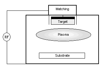
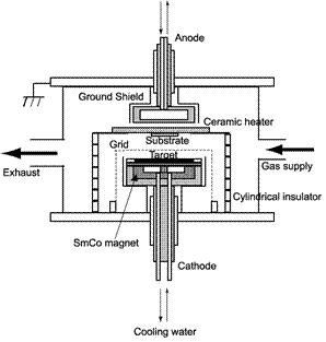
General Principle of Operation The above illustration describes a generic manifestation of a magnetron sputtering source DC, pulsed DC, AC and RF power supplies may be used, depending upon target material, if reactive sputtering is desired and other factors A permanent magnet structure is located behind a target serving as a deposition source. Magnetron sputtering is a deposition technology involving a gaseous plasma which is generated and confined to a space containing the material to be deposited – the ‘target’. RF magnetron sputtering is available in a variety of source configurations and compatible with many of Angstrom’s process control capabilities and advanced fixturing options.
MoO 3 thin films were deposited onto glass and silicon substrates held at temperature of 473 K by sputtering of pure metallic molybdenum target in oxygen and argon gas mixture using reactive RF magnetron sputtering technique Metallic molybdenum target (9999% pure) with 50 mm diameter and 3 mm thickness was used as sputter target. Aluminum oxide films were deposited on crystalline silicon substrates by reactive RF magnetron sputtering The influences of the deposition parameters on the surface passivation, surface damage, optical properties, and composition of the films have been investigated It is found that proper sputtering power and uniform magnetic field reduced the surface damage from the highenergy ion. RF magnetron operation for sputtering electrodes has some attractive attributes especially for research focussed work Both metal and dielectric materials can be sputtered Oxide islands and asperities on target sources do not lead to arcing This can be major benefit, compared to the DC case, where a system does not have vacuum load lock.
RF Magnetron Sputtering System We take pleasure in introducing ourselves as leading firm by manufacturing RF Magnetron Sputtering System to our customers Offered RF Magnetron Sputtering System is well known for efficient working. The depositions were performed with a RF magnetron sputtering PlasmalabSystem400 (Oxford Instruments, Abingdon, UK) using the parameters described in Table 1 The sputtering was made from a titanium target with a 150 mm diameter and 6 mm thickness, attached to a balanced magnetron.
Mn Coatings On The Micro Pore Formed Ti 29nb Xhf Alloys By Rf Magnetron Sputtering For

Optimization Of Rf Magnetron Sputtering Process Parameters Based On Genetic Algorithm And Neural Network Scientific Net
Ppt Rf Magnetron Sputtering System Powerpoint Presentation Free Download Id
Rf Magnetron Sputtering のギャラリー
Optimization Of Low Temperature Rf Magnetron Sputtering Of Indium Tin Oxide Films For Solar Cell Applications Applied Surface Science X Mol

Rf Magnetron Sputtering System At Rs Piece Sputtering Systems Id

Plasma Characteristics And Target Erosion Profile Of Racetrack Shaped Rf Magnetron Plasma With Weak Rubber Magnets For Full Circular Target Utilization Advanc Rubber Magnet Plasma Circular
Coatings Free Full Text Rf Dc Magnetron Sputtering Deposition Of Thin Layers For Solar Cell Fabrication
Improved Electrochromic Performance Of A Radio Frequency Magnetron Sputtered Nio Thin Film With High Optical Switching Speed Rsc Advances Rsc Publishing

What Is Rf Sputtering
Rf Sputtering

Dc Rf Magnetron Sputtering System Samwon Vacuum Komachine

2 Rf Plasma Magnetron Sputtering Coater For Non Conductive Thin Films Vtc 2rf

Growth Of Moo 3 Films By Rf Magnetron Sputtering Studies On The Structural Optical And Electrochromic Properties Topic Of Research Paper In Nano Technology Download Scholarly Article Pdf And Read For Free
Structural And Optical Properties Of A Radio Frequency Magnetron Sputtered Zno Thin Film With Different Growth Angles Nanoscale Research Letters Full Text
Aip Scitation Org Doi Pdf 10 1063 1

Principle Of The Reactive Radio Frequency Rf Magnetron Sputtering Download Scientific Diagram

Rf Magnetron Sputtering Monotarget Chilab

Sds4 Rf Magnetron Sputtering System Ceeri Pilani En

Rf Magnetron Sputtering Research Papers Academia Edu

Rf Magnetron Sputtering Laboratoire Charles Coulomb
Plasma Parameter Analysis In A Rf Magnetron Sputtering Equipment

Figure 3 Growth Of Films By Rf Magnetron Sputtering Studies On The Structural Optical And Electrochromic Properties
Www Physlab Org Wp Content Uploads 16 04 Murtaza Presentaion Pdf

Top Pdf Rf Magnetron Sputtering 1library

Magnetron Sputtering An Overview Sciencedirect Topics

Fabrication Of Oriented Hydroxyapatite Film By Rf Magnetron Sputtering Aip Advances Vol 7 No 8

Dc Rf Magnetron Sputter

Room Temperature Deposition Of Silicon Thin Films By Rf Magnetron Sputtering Scientific Net
Balanced And Unbalanced Magnetron Sputtering Vaccoat
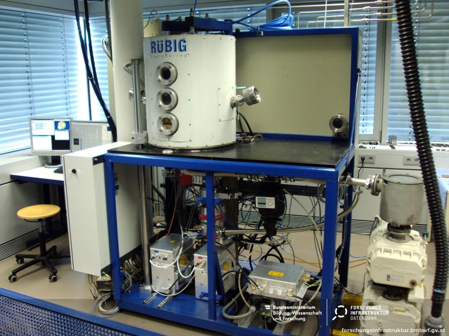
Pvd Physical Vapour Deposition Rf Magnetron Sputtering Forschungsinfrastruktur

Top Pdf Rf Magnetron Sputtering 1library
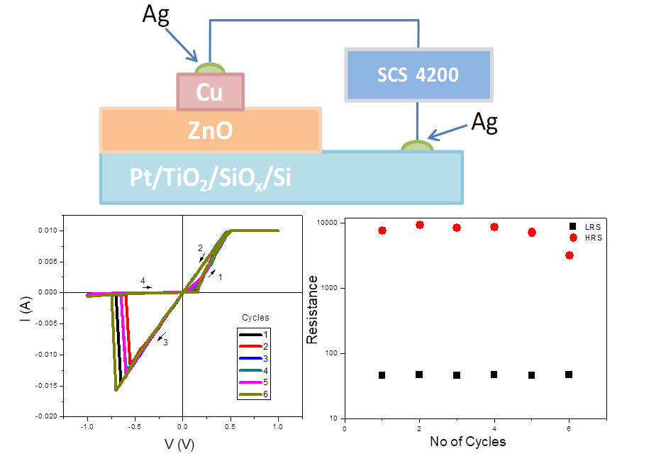
Resistive Switching Behaviour Of Rf Magnetron Sputtered Zno Thin Films
Advances In Rf Sputtering Aultimut

Study Of Zno Al Thin Films Prepared By Rf Magnetron Sputtering Under Different Ar Flow By International Journal For Scientific Research And Development Ijsrd Issuu

Rf Magnetron Sputtering Research Papers Academia Edu

The Influence Of Annealing On The Properties Of Zno Al Layers Obtained By Rf Magnetron Sputtering Sciencedirect

Rf Magnetron Sputtering Nanofabrication Laboratory

Figure 1 Growth Of Films By Rf Magnetron Sputtering Studies On The Structural Optical And Electrochromic Properties

Figure 1 From Growth Of Rm Mgb 2 Thin Films In Situ By Rf Magnetron Sputtering With A Pocket Heater Semantic Scholar

Schematic Of Rf Magnetron Sputtering 1 Substrate Stage 2 Glass Download Scientific Diagram

Rf Sputtering Principles Ifn Trento

Schematic Diagram Of Rf Magnetron Sputter System Download Scientific Diagram

Optimization Of Sputtering Parameters For The Deposition Of Low Resistivity Indium Tin Oxide Thin Films
The Optical And Electrical Properties Of Zno Al Thin Films Deposited At Low Temperatures By Rf

China Rf Magnetron Sputtering Deposition System Manufacturers Company
Single Target Rf Magnetron Sputtering Coater
Rf Magnetron Sputtering Of Thick Film Amorphous Beryllium Unt Digital Library
Q Tbn And9gcsmv5sez6h2h0cqzl7jqe7m54c0p2spndvowf Wnheskv3v Wsg Usqp Cau
Anelva Rf Magnetron Sputtering Unit Model Spf 332h

What Is Dc Sputtering

Radio Frequency Magnetron Sputter Deposition As A Tool For Surface Modification Of Medical Implants Intechopen
Evidence Of Magnetism In Rf Magnetron Sputtered Deposited Carbon Films And Investigation Of Its Origin Carbon X Mol

Radio Frequency Magnetron Sputter Deposition As A Tool For Surface Modification Of Medical Implants Intechopen

What Is Rf Sputtering
1

Magnetron Sputtering System Market Size Analysis Trends And Forecast To 27

63 Xps Analysis Of Rf Magnetron Sputtered Calcium Phosphate Coating

Figure 1 From Surface Properties And Biocompatibility Of Nanostructured Tio2 Film Deposited By Rf Magnetron Sputtering Semantic Scholar

Comparison Of Ito Prepared By Capacitive Rf Magnetron Sputtering And Dc Facing Target Sputtering As An Anode On The Organic Light Emitting Diode Kim 09 Physica Status Solidi A Wiley Online Library
Combined Magnetron Sputtering And Pulsed Laser Deposition Of Tio 2 And Bfco Thin Films Scientific Reports

Rf Sputtering Principles Ifn Trento

Rf Magnetron Sputtering Youtube

Research Center For Magnetic And Spintronic Materials
Www Jove Com Pdf Jove Protocol Radio Frequency Magnetron Sputtering Gdba2cu3o7 La067sr033mno3 Quasi Language Spanish

Physical Analysis Of Vo2 Films Grown By Atomic Layer Deposition And Rf Magnetron Sputtering Topic Of Research Paper In Nano Technology Download Scholarly Article Pdf And Read For Free On Cyberleninka Open

Pulsed Dc Magnetron Sputtering Dc Sputtering Process Vaccoat
Q Tbn And9gcrybvcmzt70 Lkqzvntsnn 8rg3osu8vfu9poc1sfswyoiypj7e Usqp Cau
Rf Magnetron Sputtering Of Thick Platinum Coatings On Glass Microspheres Unt Digital Library
Q Tbn And9gcrmgxpgzucw S3sp1bixoax2godwfl3pff9llex4tglrv55bg8c Usqp Cau

Rf Magnetron Sputtering Ppt
Coatings Free Full Text Recent Developments In R F Magnetron Sputtered Thin Films For Ph Sensing Applications An Overview Html

Dc Rf Magnetron Sputtering System Radio Frequency Pvd Deposition Coating Machine Buy Rf Mangeton Sputtering System Rf Magnetron Sputtering Coating Machine Dc Magnetron Sputtering System Product On Alibaba Com

Fission Rf Dc Sputtering Korvus Technology

1 Schematic Representation Of A Rf Magnetron Sputtering System Download Scientific Diagram

China Three Target Heads Rf Magnetron Sputtering Coater Cy Msp300s 3rf China Rf Magnetron Sputtering Coater Magnetron Sputtering Coater
Polytetrafluoroethylene Sputtered Pes Membranes For Membrane Distillation Influence Of Rf Magnetron Sputtering Conditions Springerlink

China 1 Magnetron Sputtering Source With Flexible Head For Diy Rf Dc Sputtering Coater China Magnetron Sputtering Source Magnetron Sputtering Cathode
Coatings Free Full Text Generation Of Charged Ti Nanoparticles And Their Deposition Behavior With A Substrate Bias During Rf Magnetron Sputtering

3 Heads Compact 1 Rf Plasma Magnetron Sputtering Coater With Dc Magnetron Sputtering Option Vtc 3rf
2
More About Rf Sputtering

Dc Rf Magnetron Sputtering System Facility For Thin Film Deposition
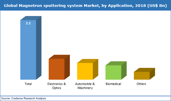
Magnetron Sputtering System Market Size Analysis Trends And Forecast To 27

Characterization Of Hafnium Diboride Thin Film Resistors By R F Magnetron Sputtering Pdf Document

Se2 Thin Films By Rf Magnetron Sputtering

Adnanotek Magnetron Sputtering Deposition Sputter System E Beam Evaporator Pld Pulsed Laser Deposition

Sputtering Sources
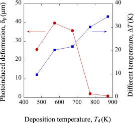
Photoinduced Deformation Of A C Thin Films Prepared By Rf Magnetron Sputtering Diamond And Related Materials X Mol

Magnetron Sputtering System Facility

Characteriztaion Of Dlc Coatings Depsotied By Rf Magnetron Sputtering Pdf Atomic Force Microscopy Carbon
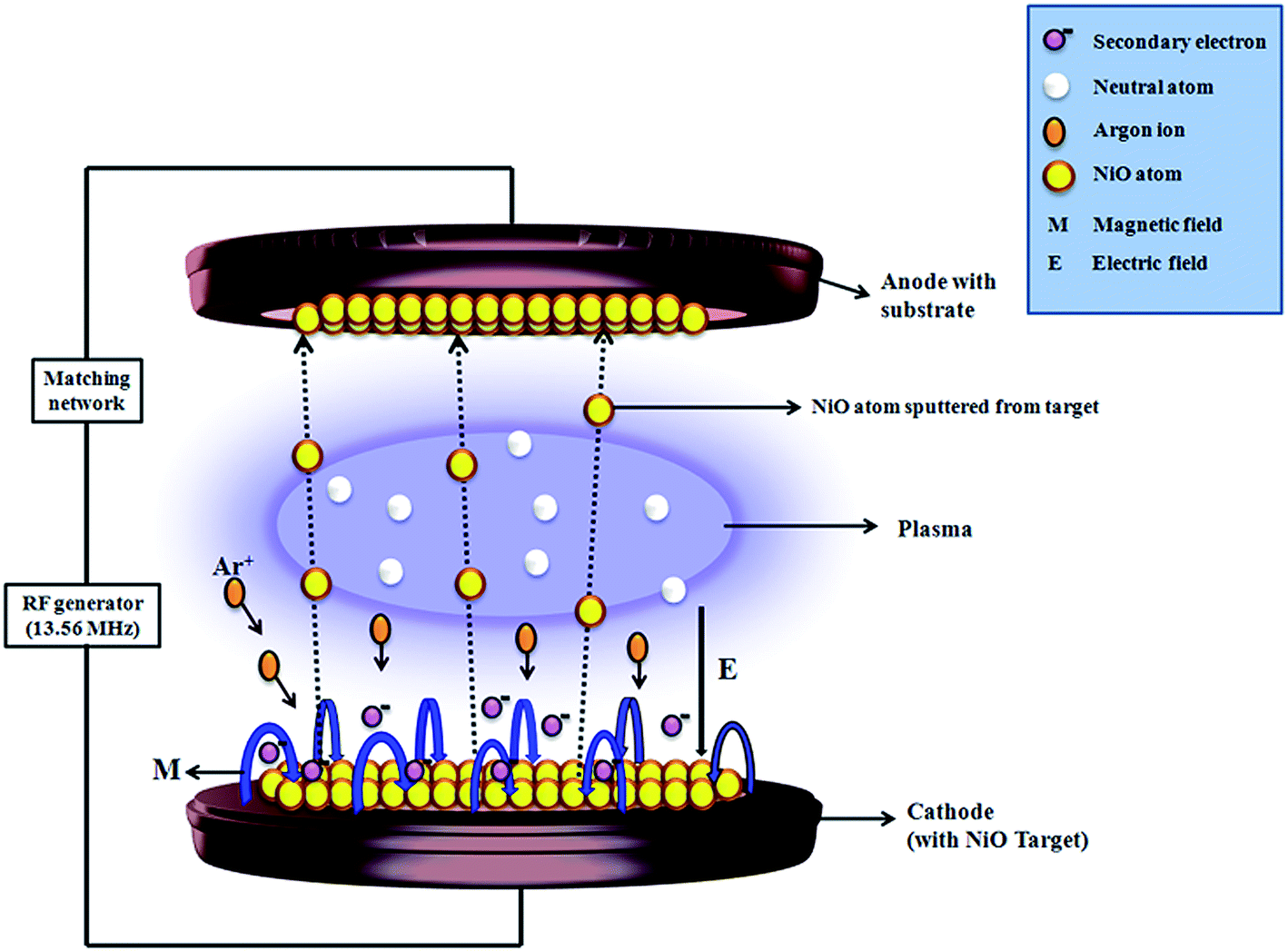
Improved Electrochromic Performance Of A Radio Frequency Magnetron Sputtered Nio Thin Film With High Optical Switching Speed Rsc Advances Rsc Publishing Doi 10 1039 C5rae

Development Of Rf Magnetron Sputtering Method To Fabricate Pzt Thin Film Actuator Sciencedirect

Schematic Representation Of Rf Magnetron Sputtering Download Scientific Diagram
Rf Magnetron Sputtering Laboratoire Charles Coulomb
Characteristics Of Al F Co Doped Zno Thin Films Grown By Rf Magnetron Sputtering With A Mesh Grid Electrode
Sputtering System Aja Atc Orion 8 Polifab

A Schematic Diagram Of Facing Target Rf Magnetron Sputt Open I

Figure 1 Schematic Diagram Of The Rf Magnetron Sputtering Chamber

Influence Of The Substrate Bias Voltage On The Crystallographic Structure And Surface Composition Of Ti6a14v Thin Films Deposited By Rf Magnetron Sputtering
Osa Optoelectronic Properties And Anisotropic Stress Of Mo Zno Thin Films Deposited On Flexible Substrates By Radio Frequency Magnetron Sputtering

Toyama
4 0 Thin Film Deposition Growth And Study Of Magnetostrictive Fesibc Thin Films For Device Applications

Preparation And Characterization Of R F Magnetron Sputtered Mo Zno Thin Films A Paper In The Materials Science An Indian Journal Materialscien Materials Plasma Mike B Hopkins
Effects Of Various Deposition Times And Rf Powers On Cdte Thin Film Growth Using Magnetron Sputtering Springerlink


